Practical Reverse Engineering Part 1 - Hunting for Debug Ports
08 Apr 2016- Part 1: Hunting for Debug Ports
- Part 2: Scouting the Firmware
- Part 3: Following the Data
- Part 4: Dumping the Flash
- Part 5: Digging Through the Firmware
In this series of posts we’re gonna go through the process of Reverse Engineering a router. More specifically, a Huawei HG533.

At the earliest stages, this is the most basic kind of reverse engineering. We’re simple looking for a serial port that the engineers who designed the device left in the board for debug and -potentially- technical support purposes.
Even though I’ll be explaining the process using a router, it can be applied to tons of household embedded systems. From printers to IP cameras, if it’s mildly complex it’s quite likely to be running some form of linux. It will also probably have hidden debug ports like the ones we’re gonna be looking for in this post.
Finding the Serial Port
Most UART ports I’ve found in commercial products are between 4 and 6 pins, usually neatly aligned and sometimes marked in the PCB’s silkscreen somehow. They’re not for end users, so they almost never have pins or connectors attached.
After taking a quick look at the board, 2 sets of unused pads call my atention (they were unused before I soldered those pins in the picture, anyway):
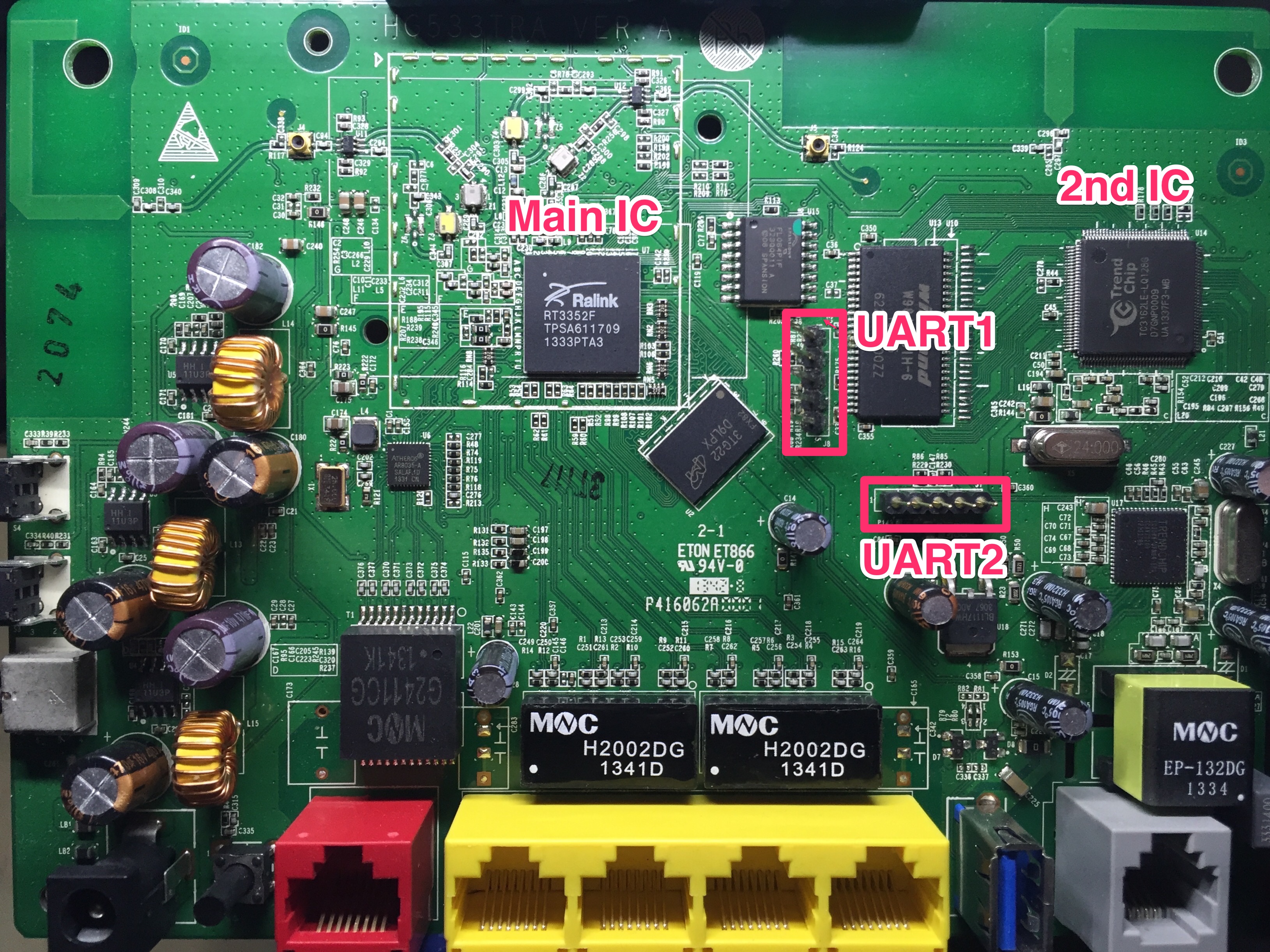
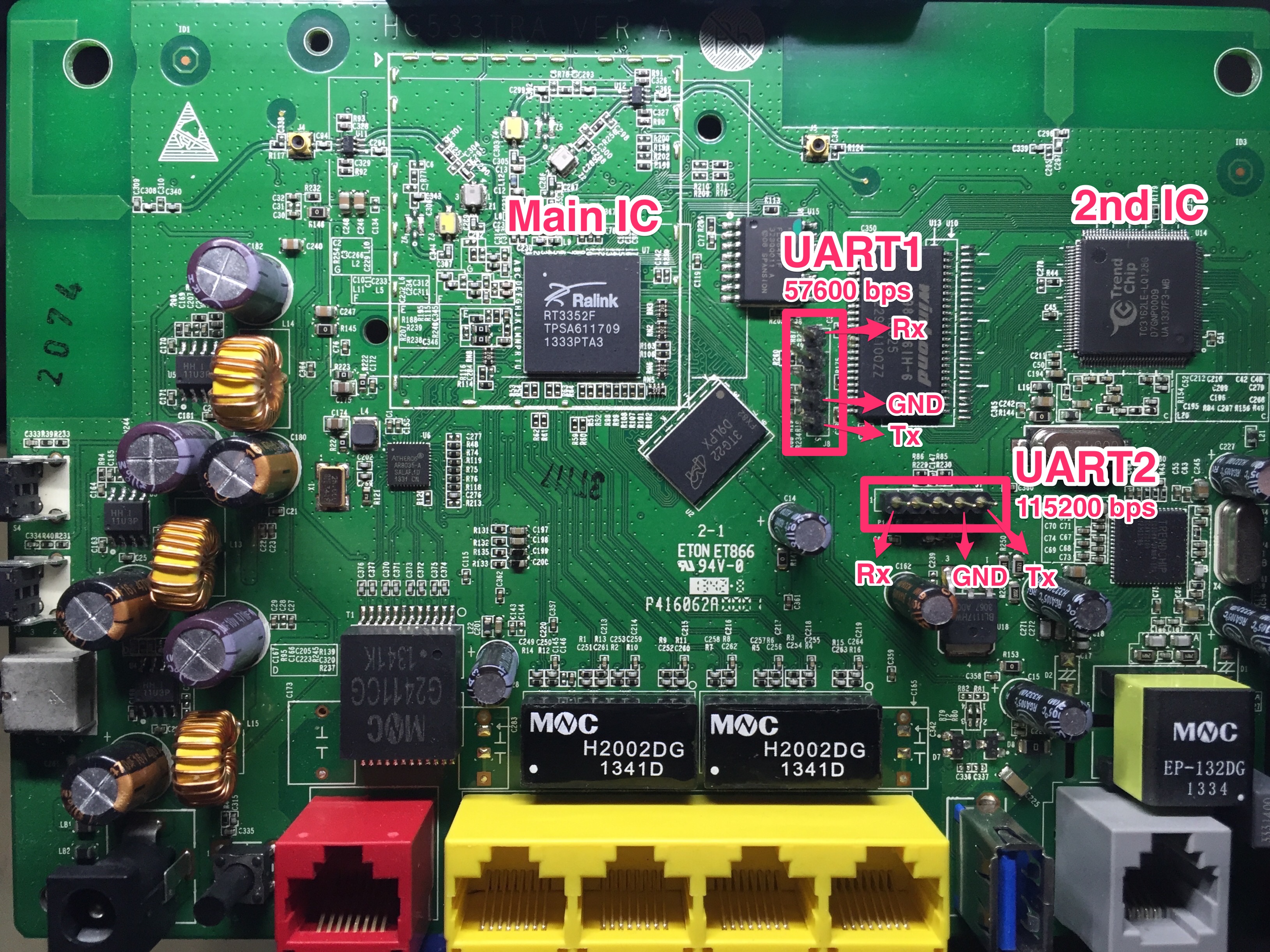
This device seems to have 2 different serial ports to communicate with 2 different Integrated Circuits (ICs). Based on the location on the board and following their traces we can figure out which one is connected to the main IC. That’s the most likely one to have juicy data.
In this case we’re simply gonna try connecting to both of them and find out what each of them has to offer.
Identifying Useless Pins
So we’ve found 2 rows of pins that -at first sight- could be UART ports. The first thing you wanna do is find out if any of those contacts is useless. There’s a very simple trick I use to help find useless pads: Flash a bright light from the backside of the PCB and look at it from directly above. This is what that looks like:
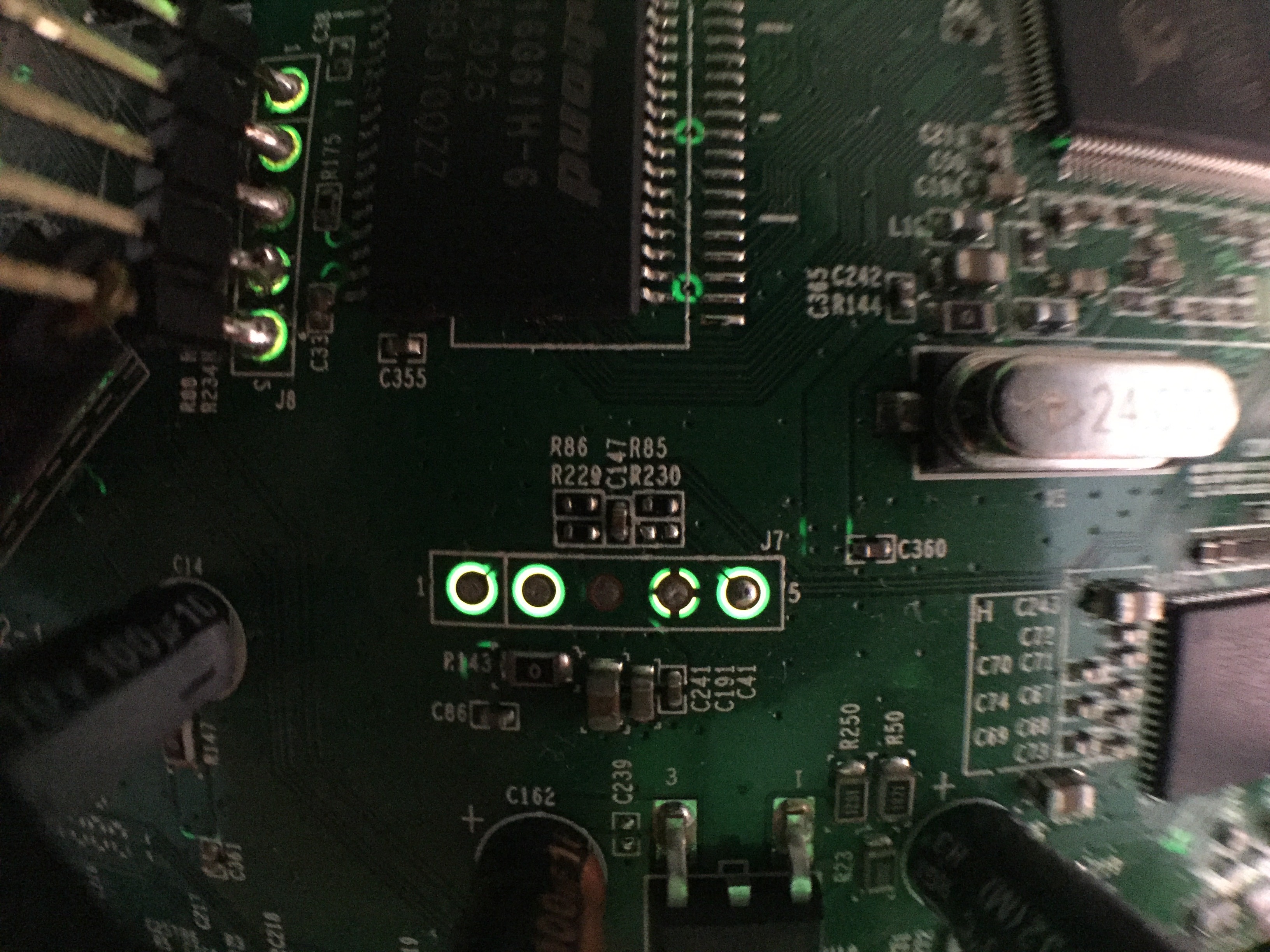
We can see if any of the layers of the PCB is making contact with the solder blob in the middle of the pad.
- Connected to something (we can see a trace “at 2 o’clock”)
- NOT CONNECTED
- 100% connected to a plane or thick trace. It’s almost certainly a power pin, either GND or Vcc
- Connections at all sides. This one is very likely to be the other power pin. There’s no reason for a data pin in a debug port to be connected to 4 different traces, but the pad being surrounded by a plane would explain those connections
- Connected to something
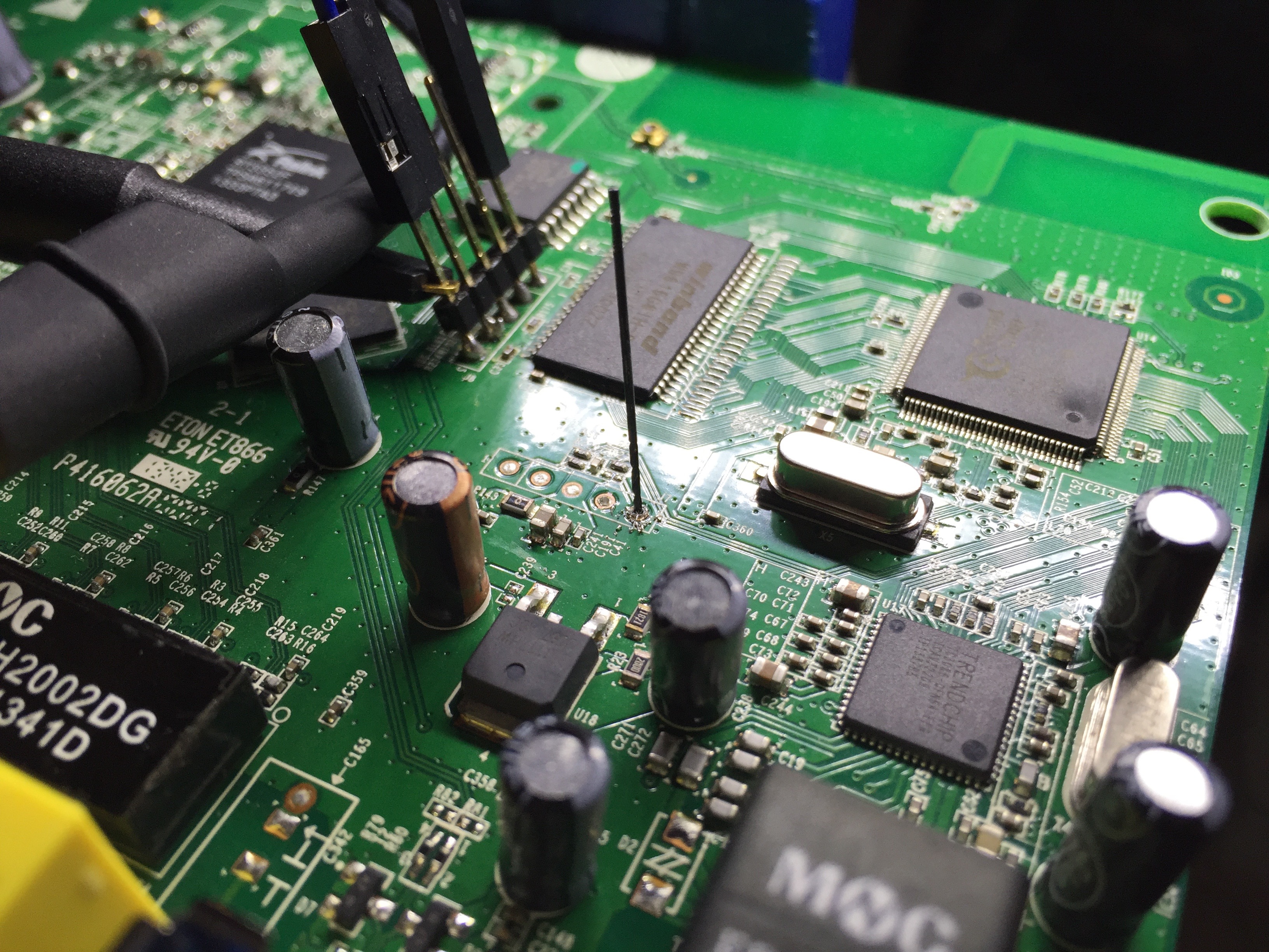
Soldering Pins for Easy Access to the Lines
In the picture above we can see both serial ports.
The pads in these ports are through-hole, but the holes themselves are filled in with blobs of very hard, very high melting point solder.
I tried soldering the pins over the pads, but the solder they used is not easy to work with. For the 2nd serial port I decided to drill through the solder blobs with a Dremel and a needle bit. That way we can pass the pins through the holes and solder them properly on the back of the PCB. It worked like a charm.
Identifying the Pinout
So we’ve got 2 connectors with only 3 useful pins each. We still haven’t verified the ports are operative or identified the serial protocol used by the device, but the number and arrangement of pins hint at UART.
Let’s review the UART protocol. There are 6 pin types in the spec:
- Tx [Transmitting Pin. Connects to our Rx]
- Rx [Receiving Pin. Connects to our Tx]
- GND [Ground. Connects to our GND]
- Vcc [The board’s power line. Usually 3.3V or 5V. DO NOT CONNECT]
- CTS [Typically unused]
- DTR [Typically unused]
We also know that according to the Standard, Tx and Rx are pulled up (set to 1) by default. The Transmitter of the line (Tx) is in charge of pulling it up, which means if it’s not connected the line’s voltage will float.
So let’s compile what we know and get to some conclusions:
- Only 3 pins in each header are likely to be connected to anything. Those must be Tx, Rx and GND
- Two pins look a lot like Vcc and GND
- One of them -Tx- will be pulled up by default and be transmitting data
- The 3rd of them, Rx, will be floating until we connect the other end of the line
That information seems enough to start trying different combinations with your UART-to-USB bridge, but randomly connecting pins you don’t understand is how you end up blowing shit up.
Let’s keep digging.
A multimeter or a logic analyser would be enough to figure out which pin is which, but if you want to understand what exactly is going on in each pin, nothing beats a half decent oscilloscope:
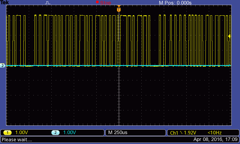
After checking the pins out with an oscilloscope, this is what we can see in each of them:
- GND and Vcc verified - solid 3.3V and 0V in pins 2 and 3, as expected
- Tx verified - You can clearly see the device is sending information
- One of the pins floats at near-0V. This must be the device’s Rx, which is floating because we haven’t connected the other side yet.
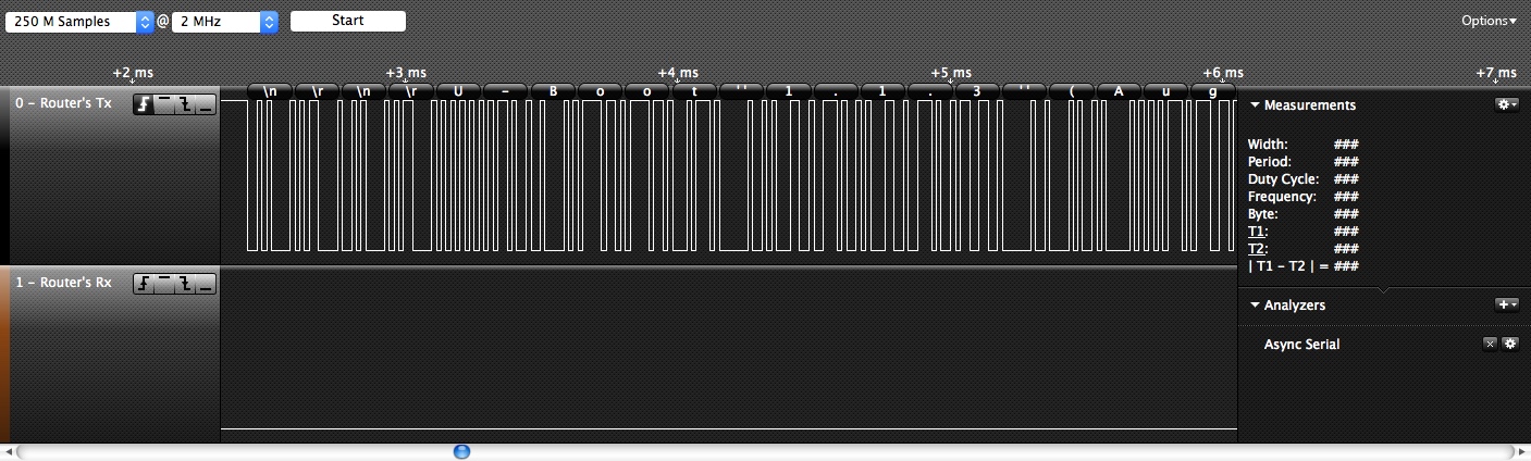
So now we know which pin is which, but if we want to talk to the serial port we need to figure out its baudrate. We can find this with a simple protocol dump from a logic analyser. If you don’t have one, you’ll have to play “guess the baudrate” with a list of the most common ones until you get readable text through the serial port.
This is a dump from a logic analyser in which we’ve enabled protocol analysis
and tried a few different baudrates. When we hit the right one, we start seeing
readable text in the sniffed serial data (\n\r\n\rU-Boot 1.1.3 (Aug...)
Once we have both the pinout and baudrate, we’re ready to start communicating with the device:
Connecting to the Serial Ports
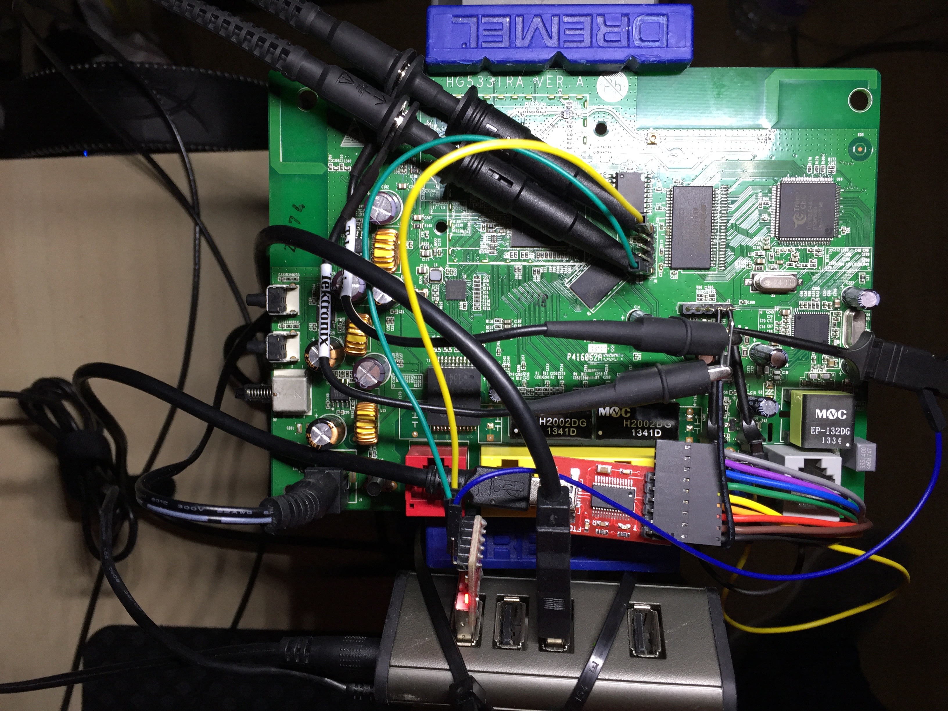
Now that we’ve got all the info we need on the hardware side, it’s time to start talking to the device. Connect any UART to USB bridge you have around and start wandering around. This is my hardware setup to communicate with both serial ports at the same time and monitor one of the ports with an oscilloscope:
And when we open a serial terminal in our computer to communicate with the device, the primary UART starts spitting out useful info. These are the commands I use to connect to each port as well as the first lines they send during the boot process:
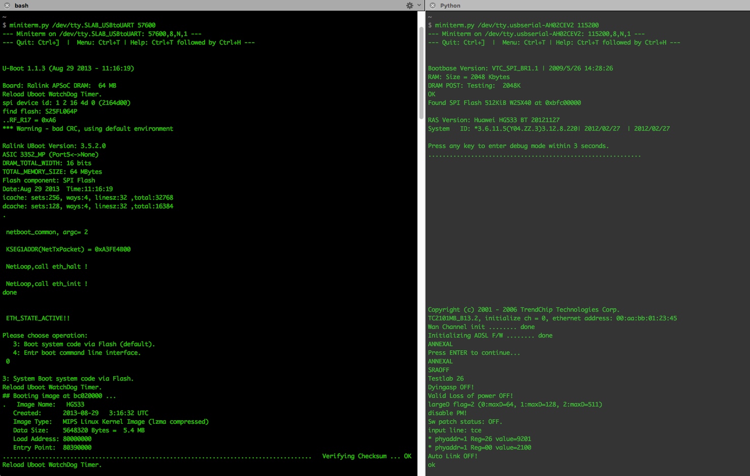
Please choose operation:
   3: Boot system code via Flash (default).
   4: Entr boot command line interface.
 0
‘Command line interface’?? We’ve found our way into the system! When we press 4
we get a command line interface to interact with the device’s bootloader.
Furthermore, if we let the device start as the default 3, wait for it to
finish booting up and press enter, we get the message Welcome to ATP Cli
and a login prompt. If the devs had modified the password this step would be a
bit of an issue, but it’s very common to find default credentials in embedded
systems. After a few manual tries, the credentials admin:admin succeeded and I
got access into the CLI:
-------------------------------
-----Welcome to ATP Cli------
-------------------------------

Login: admin
Password:    #Password is ‘admin'
ATP>shell

BusyBox vv1.9.1 (2013-08-29 11:15:00 CST) built-in shell (ash)
Enter 'help' for a list of built-in commands.

# ls
var   usr   tmp   sbin  proc  mnt   lib   init  etc   dev   bin
Running the shell command in ATP will take us directly into Linux’s CLI with
root privileges :)
This router runs BusyBox, a linux-ish interface which I’ll talk about in more detail in the next post.
Next Steps
Now that we have access to the BusyBox CLI we can start nosing around the software. Depending on what device you’re reversing there could be plain text passwords, TLS certificates, useful algorithms, unsecured private APIs, etc. etc. etc.
In the next post we’ll focus on the software side of things. I’ll explain the differences between boot modes, how to dump memory, and other fun things you can do now that you’ve got direct access to the device’s firmware.
Thanks for reading! :)