In Parts 1 to 3 we’ve been gathering data within its context. We could sniff
the specific pieces of data we were interested in, or observe the resources
used by each process. On the other hand, they had some serious limitations;
we didn’t have access to ALL the data, and we had to deal with very minimal
tools… And what if we had not been able to find a serial port on the PCB?
What if we had but it didn’t use default credentials?
In this post we’re gonna get the data straight from the source, sacrificing
context in favour of absolute access. We’re gonna dump the data from the Flash
IC and decompress it so it’s usable. This method doesn’t require expensive
equipment and is independent of everything we’ve done until now. An external
Flash IC with a public datasheet is a reverser’s great ally.
Dumping the Memory Contents
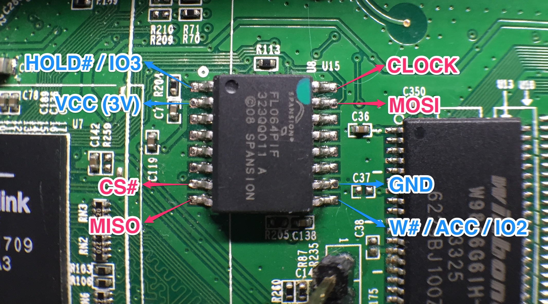
As discussed in Part 3, we’ve got access to the datasheet for the Flash IC, so
there’s no need to reverse its pinout:
We also have its instruction set, so we can communicate with the IC using almost
any device capable of ‘speaking’ SPI.
We also know that powering up the router will cause the Ralink to start
communicating with the Flash IC, which would interfere with our own attempts to
read the data. We need to stop the communication between the Ralink and the
Flash IC, but the best way to do that depends on the design of the circuit we’re
working with.
Do We Need to Desolder The Flash IC? [Theory]
The perfect way to avoid interference would be to simply desolder the Flash IC
so it’s completely isolated from the rest of the circuit. It gives us absolute
control and removes all possible sources of interference. Unfortunately, it also
requires additional equipment, experience and time, so let’s see if we can avoid
it.
The second option would be to find a way of keeping the Ralink inactive while
everything else around it stays in standby. Microcontrollers often have a Reset
pin that will force them to shut down when pulled to 0; they’re commonly used
to force IC reboots without interrupting power to the board. In this case we
don’t have access to the Ralink’s full datasheet (it’s probably distributed only
to customers and under NDA); the IC’s form factor and the complexity of the
circuit around it make for a very hard pinout to reverse, so let’s keep
thinking…
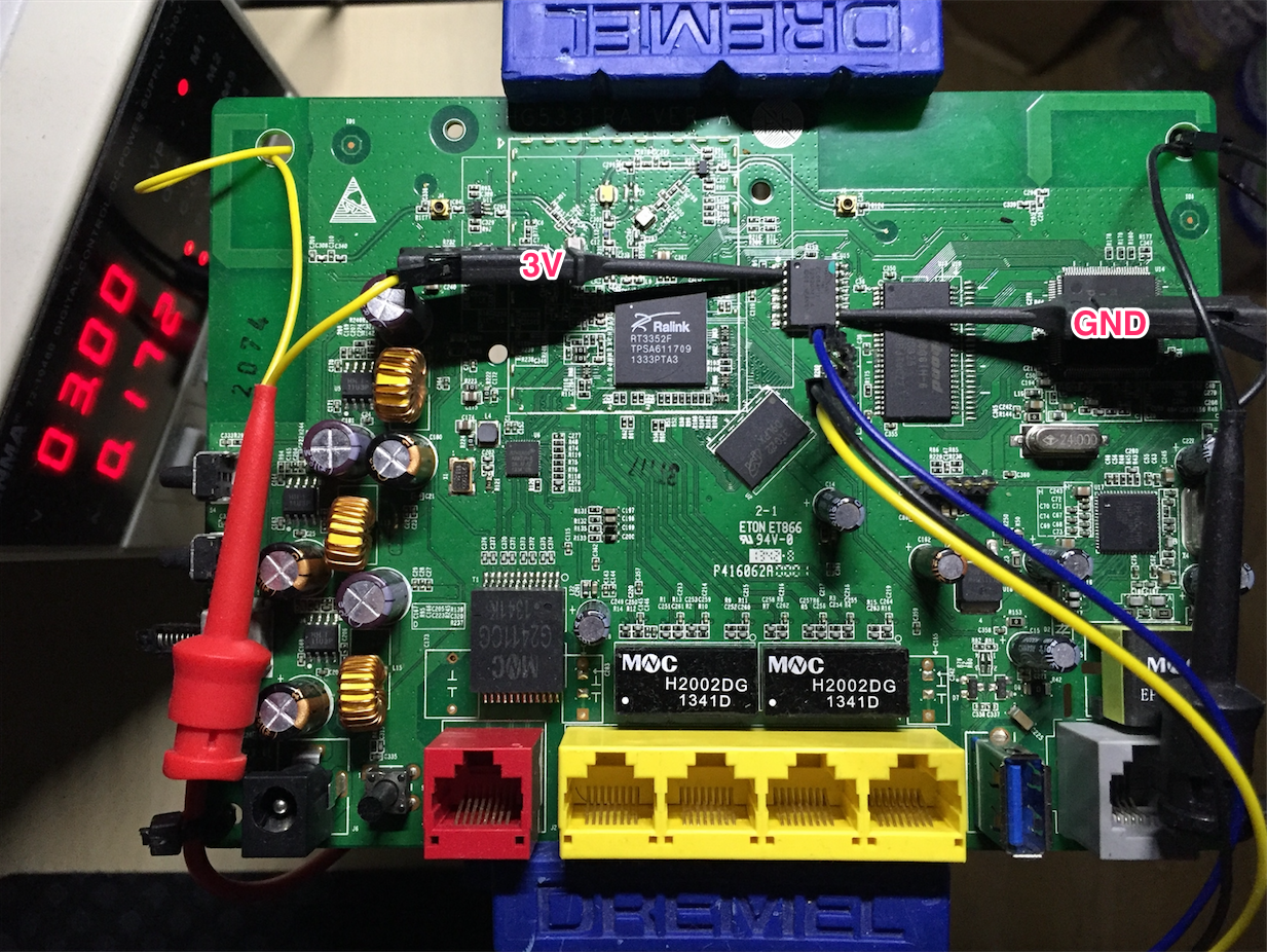
What about powering one IC up but not the other? We can try applying voltage
directly to the power pins of the Flash IC instead of powering up the whole
circuit. Injecting power into the PCB in a way it wasn’t designed for could
blow something up; we could reverse engineer the power circuit, but that’s
tedious work. This router is cheap and widely available, so I took the ‘fuck it’
approach. The voltage required, according to the
datasheet,
is 3V; I’m just gonna apply power directly to the Flash IC and see what happens.
It may power up the Ralink too, but it’s worth a try.
We start supplying power while observing the board and waiting for data from
the Ralink’s UART port. We can see some LEDs light up at the back of the PCB,
but there’s no data coming out of the UART port; the Ralink must not be running.
Even though the Ralink is off, its connection to the Flash IC may still interfere
with our traffic because of multiple design factors in both power circuit and the
silicon. It’s important to keep that possibility in mind in case we see anything
dodgy later on; if that was to happen we’d have to desolder the Flash IC (or just
its data pins) to physically disconnect it from everything else.
The LEDs and other static components can’t communicate with the Flash IC, so they
won’t be an issue as long as we can supply enough current for all of them.
I’m just gonna use a bench power supply, with plenty of current available for
everything. If you don’t have one you can try using the Master’s power lines,
or some USB power adapter if you need some more current. They’ll probably do
just fine.
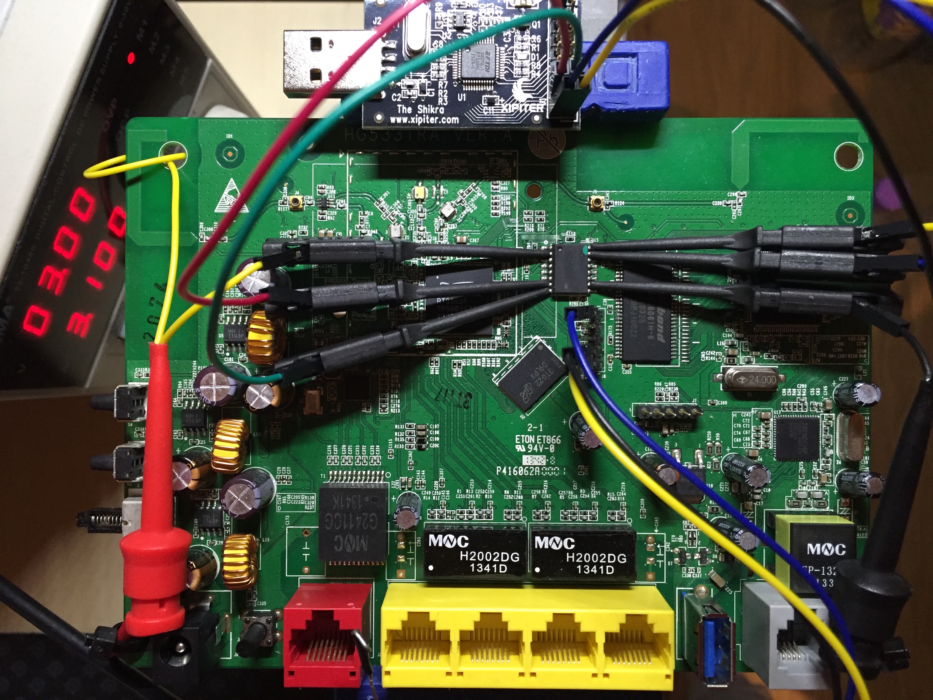
Time to connect our SPI Master.
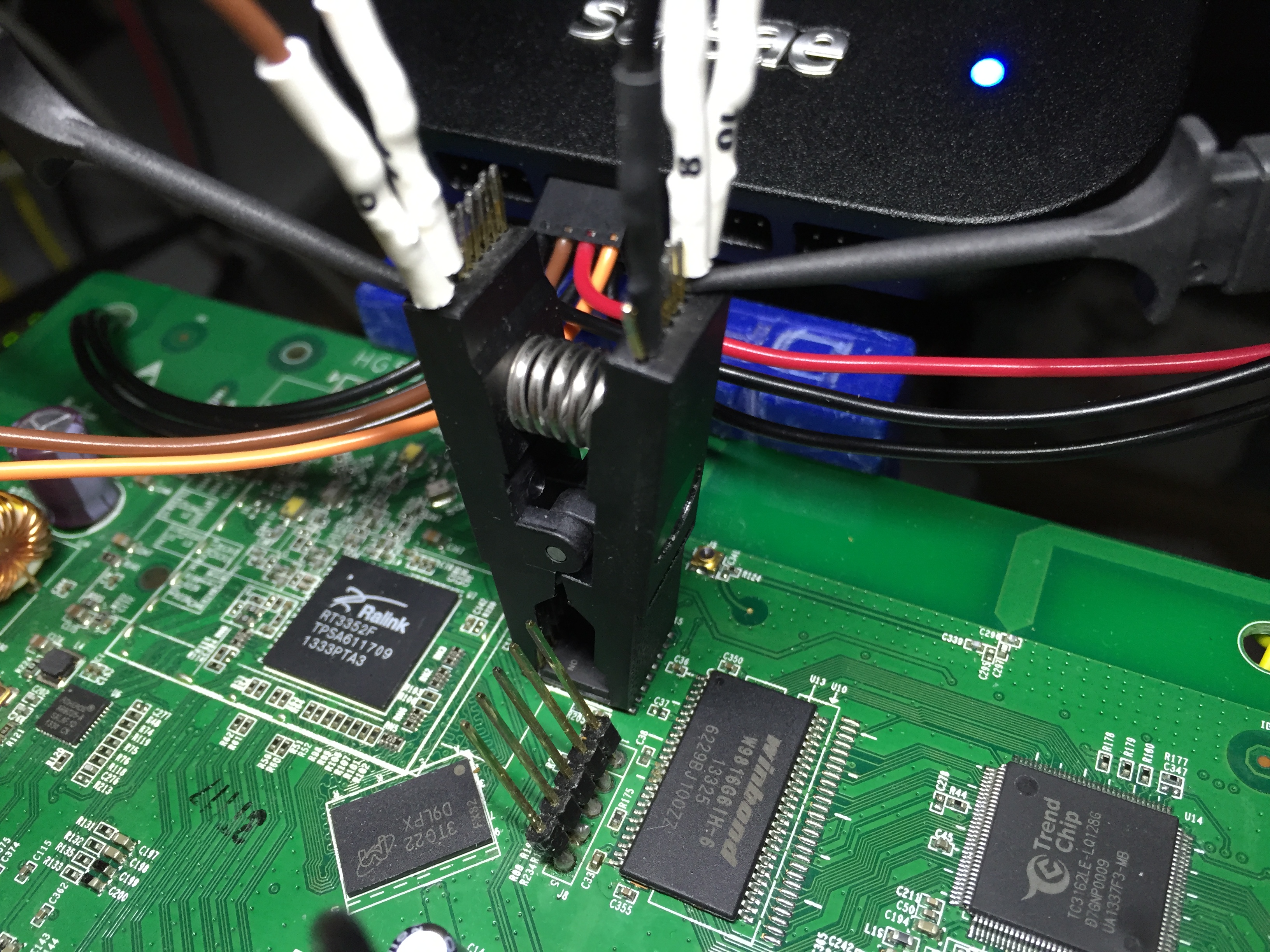
Connecting to the Flash IC
Now that we’ve confirmed there’s no need to desolder the Ralink we can connect
any device that speaks SPI and start reading memory contents block by block.
Any microcontroller will do, but a purpose-specific SPI-USB bridge will often
be much faster. In this case I’m gonna be using a board based on the FT232H,
which supports SPI among some other low level protocols.
We’ve got the pinout for both the Flash and my
USB-SPI bridge,
so let’s get everything connected.
Now that the hardware is ready it’s time to start pumping data out.
Dumping the Data
We need some software in our computer that can understand the USB-SPI bridge’s
traffic and replicate the memory contents as a binary file. Writing our own
wouldn’t be difficult, but there are programs out there that already support
lots of common Masters and Flash ICs. Let’s try the widely known and open source
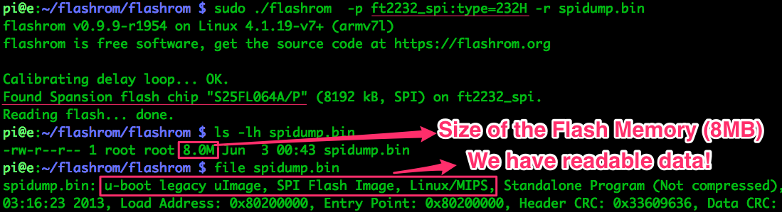
flashrom.
flashrom is old and buggy, but it already supports both the FT232H as
Master and the FL064PIF as Slave. It gave me lots of trouble in both OSX and
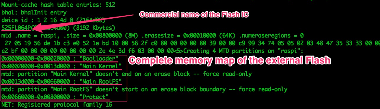
an Ubuntu VM, but ended up working just fine on a Raspberry Pi (Raspbian):
Success! We’ve got our memory dump, so we can ditch the hardware and start
preparing the data for analysis.
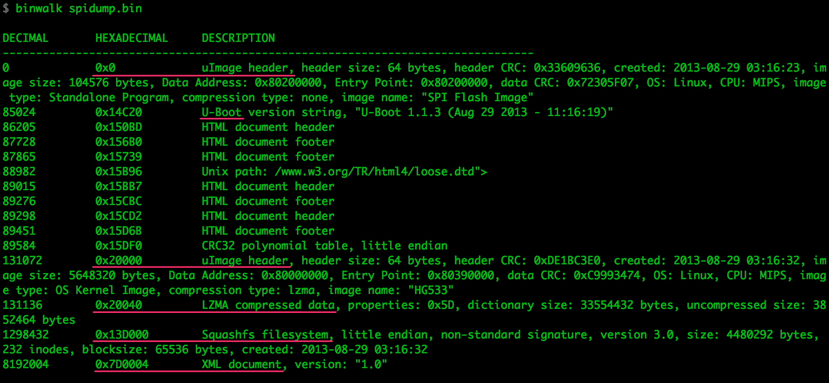
Splitting the Binary
The file command has been able to identify some data about the binary, but
that’s just because it starts with a header in a supported format. In a
0-knowledge scenario we’d use binwalk
to take a first look at the binary file and find the data we’d like to extract.
Binwalk is a very useful tool for binary analysis created by the
awesome hackers at /dev/ttyS0; you’ll certainly get
to know them if you’re into hardware hacking.
In this case we’re not in a 0-knowledge scenario; we’ve been gathering data since
day 1, and we obtained a complete memory map of the Flash IC in Part 2. The
addresses mentioned in the debug message are confirmed by binwalk, and it makes
for much cleaner splitting of the binary, so let’s use it:
With the binary and the relevant addresses, it’s time to split the binary into
its 4 basic segments. dd takes its parameters in terms of block size (bs,
bytes), offset (skip, blocks) and size (count, blocks); all of them in
decimal. We can use a calculator or let the shell do the hex do decimal
conversions with $(()):
$ dd if=spidump.bin of=bootloader.bin bs=1 count=$((0x020000))
131072+0 records in
131072+0 records out
131072 bytes transferred in 0.215768 secs (607467 bytes/sec)
$ dd if=spidump.bin of=mainkernel.bin bs=1 count=$((0x13D000-0x020000)) skip=$((0x020000))
1167360+0 records in
1167360+0 records out
1167360 bytes transferred in 1.900925 secs (614101 bytes/sec)
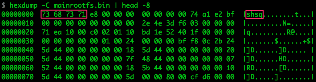
$ dd if=spidump.bin of=mainrootfs.bin bs=1 count=$((0x660000-0x13D000)) skip=$((0x13D000))
5386240+0 records in
5386240+0 records out
5386240 bytes transferred in 9.163635 secs (587784 bytes/sec)
$ dd if=spidump.bin of=protect.bin bs=1 count=$((0x800000-0x660000)) skip=$((0x660000))
1703936+0 records in
1703936+0 records out
1703936 bytes transferred in 2.743594 secs (621060 bytes/sec)
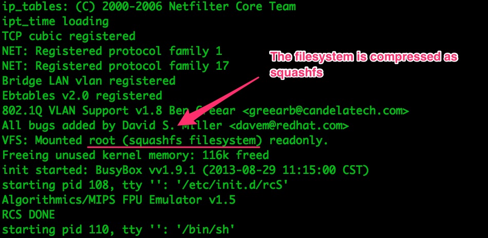
We have created 4 different binary files:
bootloader.bin:
U-boot. The bootloader.
It’s not compressed because the Ralink wouldn’t know how to decompress it.
mainkernel.bin:
Linux Kernel. The basic firmware in charge of controlling the bare metal.
Compressed using lzma
mainrootfs.bin:
Filesystem. Contains all sorts of important binaries and configuration files.
Compressed as squashfs using the lzma algorithm
protect.bin:
Miscellaneous data as explained in Part 3.
Not compressed
Extracting the Data
Now that we’ve split the binary into its 4 basic segments, let’s take a closer
look at each of them.
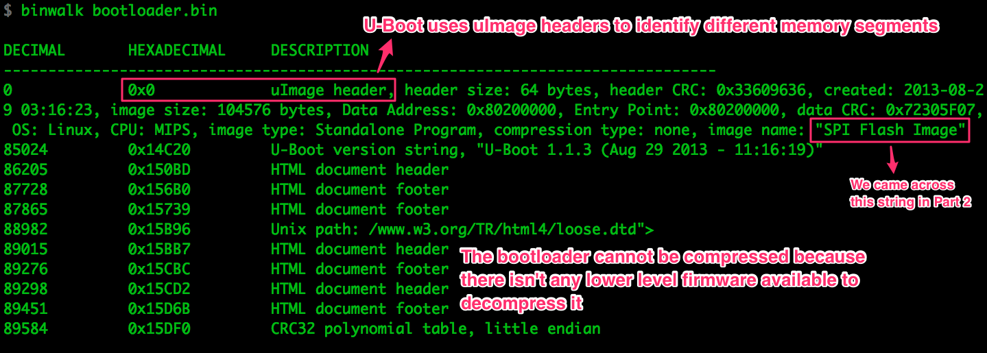
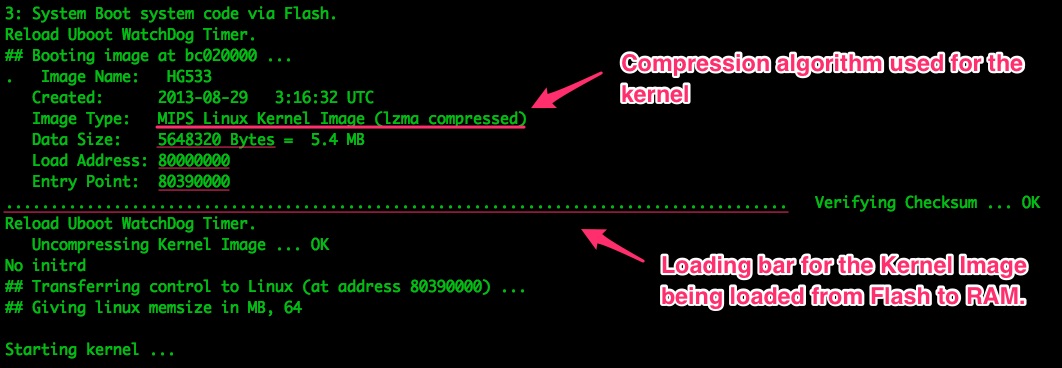
Bootloader
Binwalk found the uImage header and decoded it for us. U-Boot uses these headers
to identify relevant memory areas. It’s the same info that the file command
displayed when we fed it the whole memory dump because it’s the first header in
the file.
We don’t care much for the bootloader’s contents in this case, so let’s ignore
it.
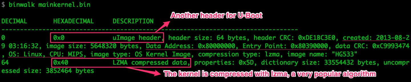
Kernel
Compression is something we have to deal with before we can make any use of the
data. binwalk has confirmed what we discovered in Part 2, the kernel
is compressed using lzma, a very popular compression algorithm in embedded
systems. A quick check with strings mainkernel.bin | less confirms there’s no
human readable data in the binary, as expected.
There are multiple tools that can decompress lzma, such as 7z or
xz. None of those liked mainkernel.bin:
$ xz --decompress mainkernel.bin
xz: mainkernel.bin: File format not recognized
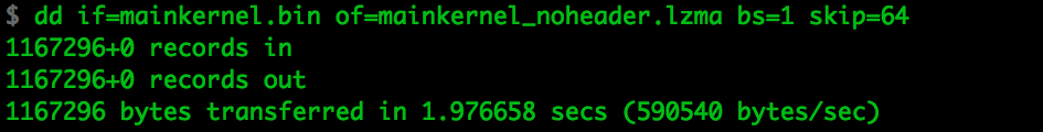
The uImage header is probably messing with tools, so we’re gonna have to strip
it out. We know the lzma data starts at byte 0x40, so let’s copy everything
but the first 64 bytes.
And when we try to decompress…
$ xz --decompress mainkernel_noheader.lzma
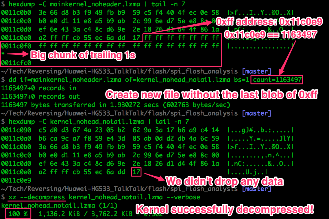
xz: mainkernel_noheader.lzma: Compressed data is corrupt
xz has been able to recognize the file as lzma, but now it doesn’t like the
data itself. We’re trying to decompress the whole mainkernel Flash area, but
the stored data is extremely unlikely to be occupying 100% of the memory segment.
Let’s remove any unused memory from the tail of the binary and try again:
xz seems to have decompressed the data successfully. We can easily verify that
using the strings command, which finds ASCII strings in binary files. Since
we’re at it, we may as well look for something useful…
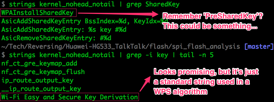
The Wi-Fi Easy and Secure Key Derivation string looks promising, but as it
turns out it’s just a hardcoded string defined by the
Wi-Fi Protected Setup spec.
Nothing to do with the password generation algorithm we’re interested in.
We’ve proven the data has been properly decompressed, so let’s keep moving.
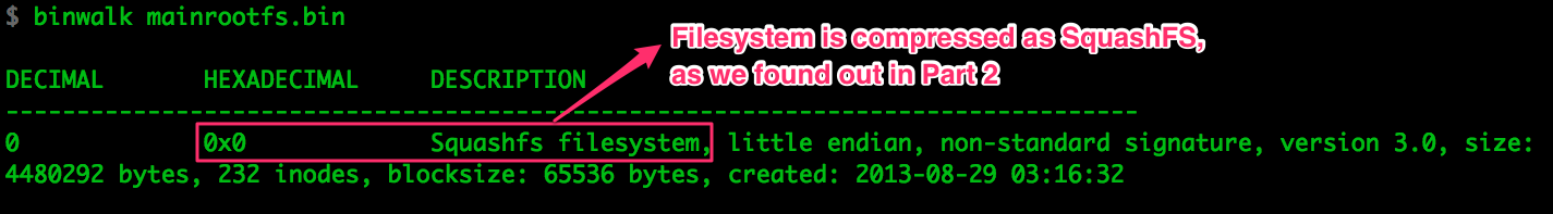
Filesystem
The mainrootfs memory segment does not have a uImage header because it’s
relevant to the kernel but not to U-Boot.
SquashFS is a very common filesystem in embedded systems. There are multiple
versions and variations, and manufacturers sometimes use custom signatures to
make the data harder to locate inside the binary. We may have to fiddle with
multiple versions of unsquashfs and/or modify the signatures, so let me show
you what the signature looks like in this case:
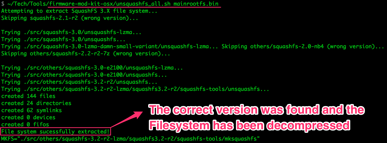
Since the filesystem is very common and finding the right configuration is
tedious work, somebody may have already written a script to automate the task.
I came across this
OSX-specific fork
of the
Firmware Modification Kit,
which compiles multiple versions of unsquashfs and includes a neat script
called unsquashfs_all.sh to run all of them. It’s worth a try.
Wasn’t that easy? We got lucky with the SquashFS version and supported signature,
and unsquashfs_all.sh managed to decompress the filesystem. Now we’ve got
every binary in the filesystem, every symlink and configuration file, and
everything is nice and tidy:
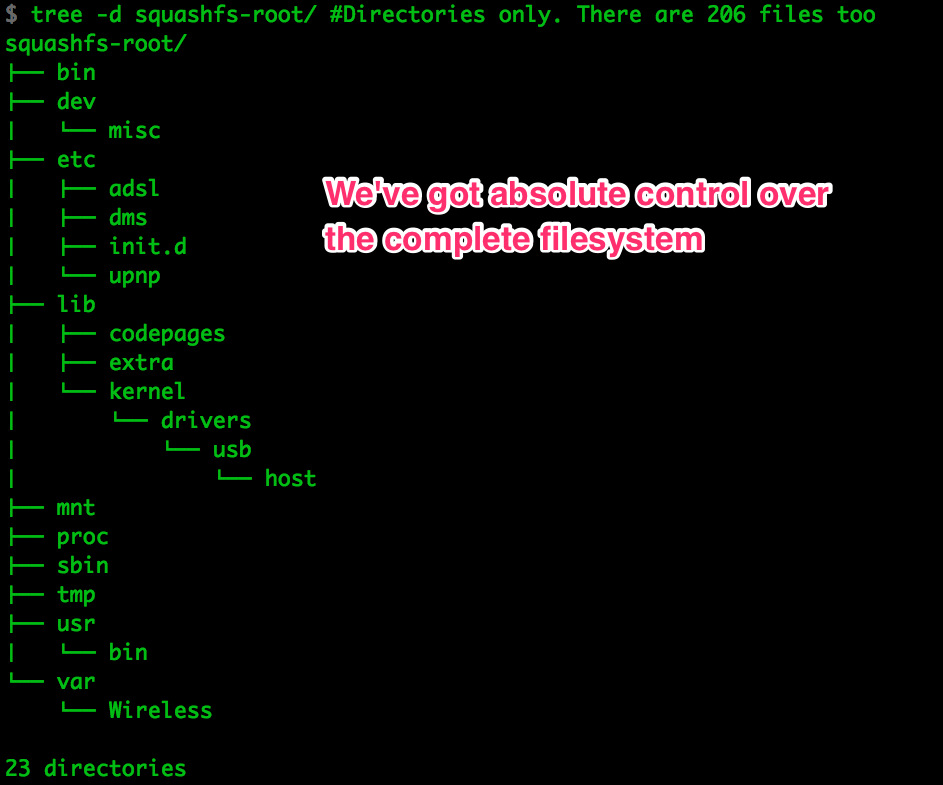
In the complete
file tree
we can see we’ve got every file in the system, (other than runtime files like
those in /var/, of course).
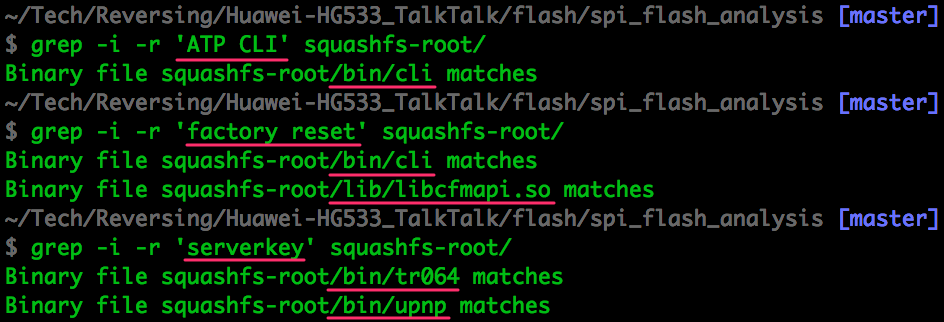
Using the intel we have been gathering on the firmware since day 1 we can start
looking for potentially interesting binaries:
If we were looking for network/application vulnerabilities in the router, having
every binary and config file in the system would be massively useful.
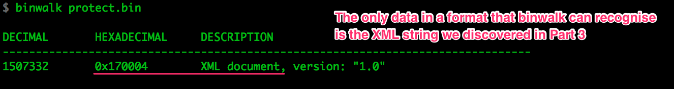
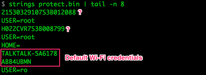
Protected
As we discussed in Part 3, this memory area is not compressed and contains all
pieces of data that need to survive across reboots but be different across
devices. strings seems like an appropriate tool for a quick overview of the
data:
Everything in there
seems to be just the curcfg.xml contents, some logs and those few isolated
strings in the picture. We already sniffed and analysed all of that data in Part
3, so there’s nothing else to discuss here.
Next Steps
At this point all hardware reversing for the Ralink is complete and we’ve
collected everything there was to collect in ROM. Just think of what you may be
interested in and there has to be a way to find it. Imagine we wanted to control
the router through the UART debug port we found in Part 1, but when we try to
access the ATP CLI we can’t figure out the credentials. After dumping the
external Flash we’d be able to find the XML file in the protect area, and
discover the credentials just like we did in Part 2
(The Rambo Approach to Intel Gathering, admin:admin).
If you couldn’t dump the memory IC for any reason, the firmware upgrade files
provided by the manufacturers will sometimes be complete memory segments;
the device simply overwrites the relevant flash areas using code previously
loaded to RAM. Downloading the file from the manufacturer would be the equivalent
of dumping those segments from flash, so we just need to decompress them.
They won’t have all the data, but it may be enough for your purposes.
Now that we’ve got the firmware we just need to think of anything we may be
interested in and start looking for it through the data. In the next post we’ll
dig a bit into different binaries and try to find more potentially useful data.
The best thing about hardware hacking is having full access to very bare metal,
and all the electrical signals that make the system work. With ingenuity and
access to the right equipment we should be able to obtain any data we want. From
simply sniffing traffic with a cheap logic analyser to using thousands of
dollars worth of equipment to obtain private keys by measuring the power
consumed by the device with enough precision (power analysis side channel
attack); if the physics make sense, it’s likely to work given the right
circumstances.
In this post I’d like to discuss traffic sniffing and how we can use it to gather
intel.
Traffic sniffing at a practical level is used all the time for all sorts of
purposes, from regular debugging during the delopment process to reversing the
interface of gaming controllers, etc. It’s definitely worth a post of its own,
even though this device can be reversed without it.
Please check out the
legal disclaimer
in case I come across anything sensitive.
Full disclosure: I’m in contact with Huawei’s security team. I tried to contact
TalkTalk, but their security staff is nowhere to be seen.
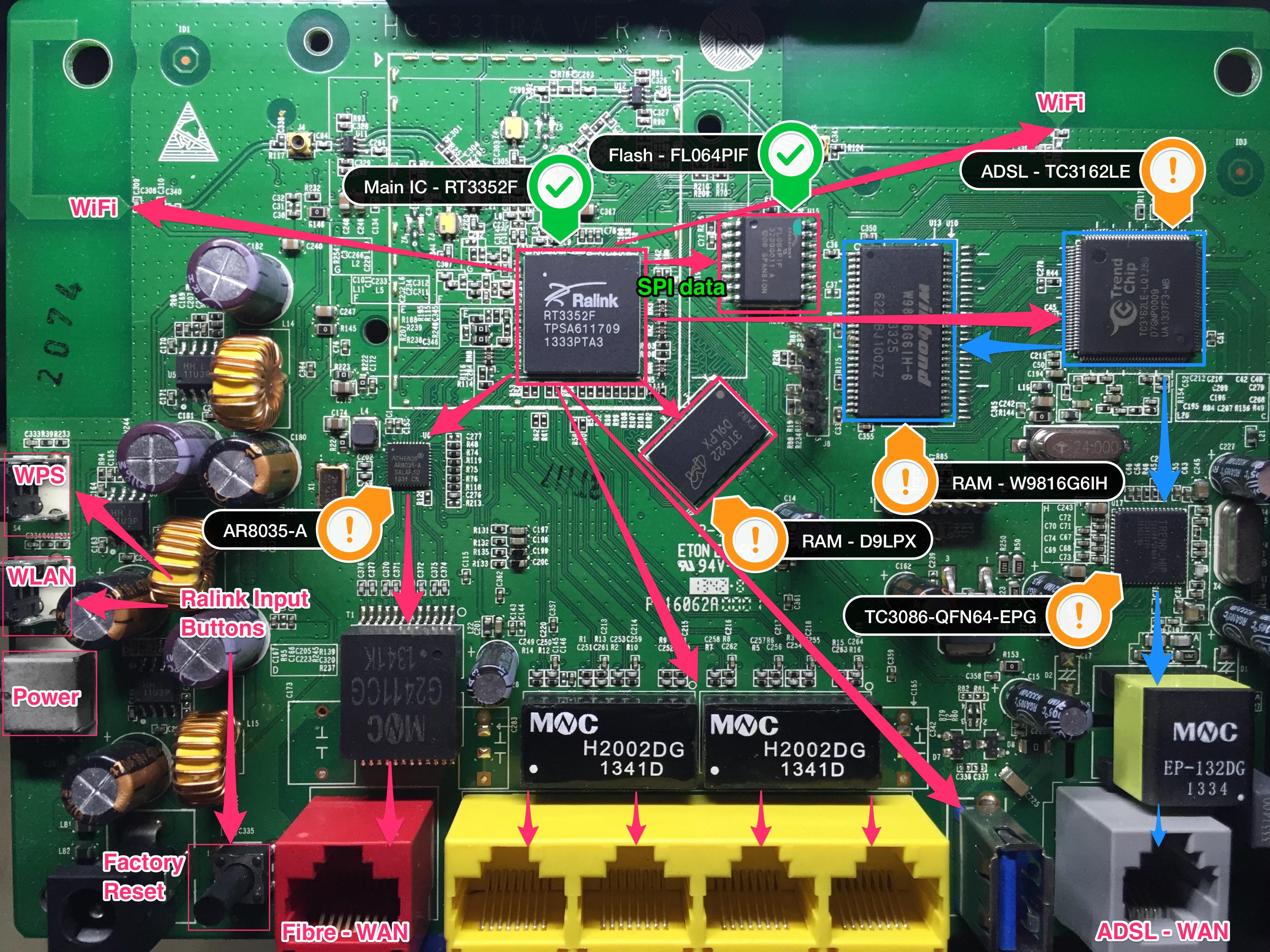
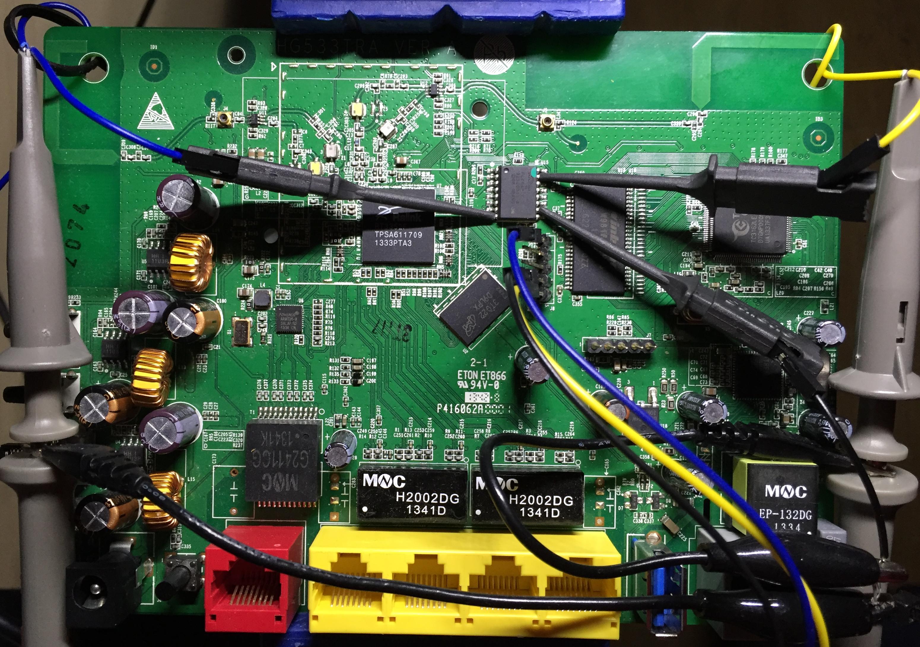
Data Flows In the PCB
Data is useless within its static memory cells, it needs to be read, written
and passed around in order to be useful. A quick look at the board is enough to
deduce where the data is flowing through, based on IC placement and PCB traces:
We’re not looking for hardware backdoors or anything buried too deep, so we’re
only gonna look into the SPI data flowing between the Ralink and its external
Flash.
Pretty much every IC in the market has a datasheet documenting all its technical
characteristics, from pinouts to power usage and communication protocols. There
are tons of public datasheets on google, so find the ones relevant to the traffic
you want to sniff:
Now we’ve got pinouts, electrical characteristics, protocol details… Let’s
take a first look and extract the most relevant pieces of data.
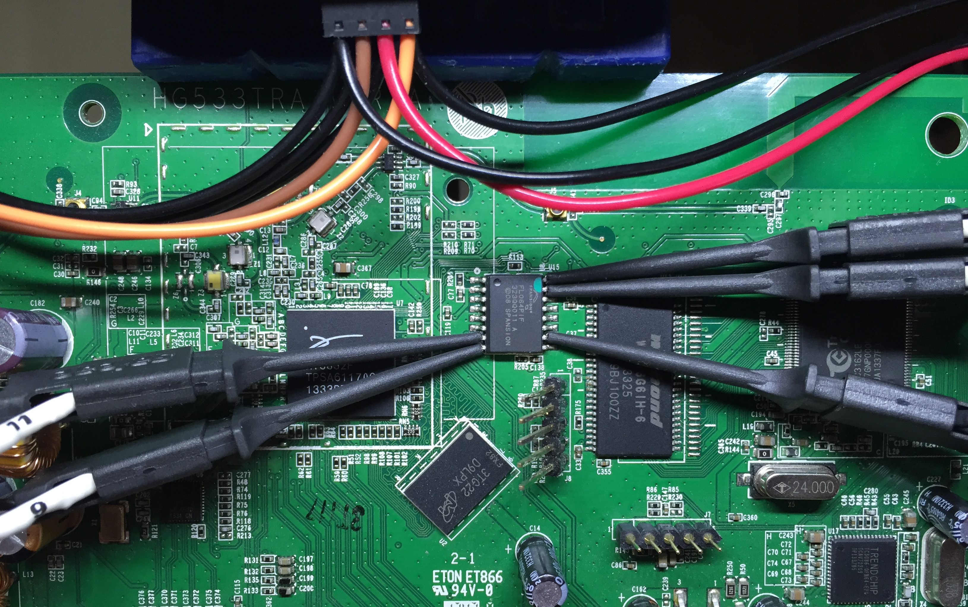
Understanding the Flash IC
We know which data flow we’re interested: The SPI traffic between the Ralink IC
and Flash. Let’s get started; the first thing we need is to figure out how to
connect the logic analyser. In this case we’ve got the datasheet for the Flash
IC, so there’s no need to reverse engineer any pinouts:
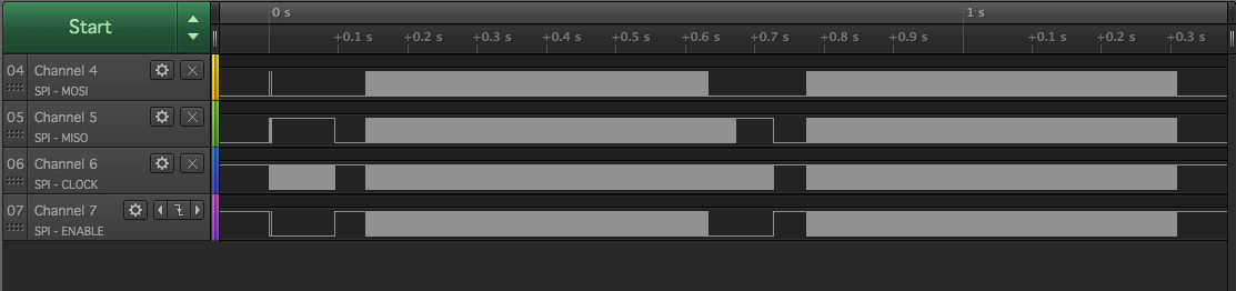
Standard SPI communication uses 4 pins:
MISO (Master In Slave Out): Data line Ralink<-Flash
MOSI (Master Out Slave In): Data line Ralink->Flash
SCK (Clock Signal): Coordinates when to read the data lines
CS# (Chip Select): Enables the Flash IC when set to 0 so multiple of them
can share MISO/MOSI/SCK lines.
We know the pinout, so let’s just connect a logic analyser to those 4 pins and
capture some random transmission:
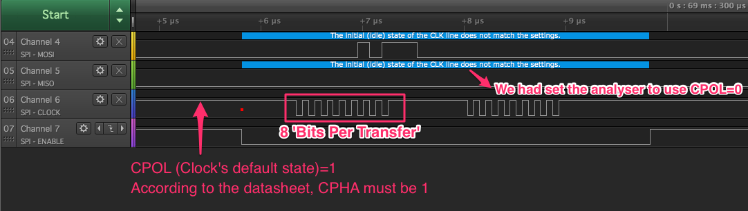
In order to set up our logic analyser we need to find out some SPI configuation
options, specifically:
Transmission endianness [Standard: MSB First]
Number of bits per transfer [Standard: 8]. Will be obvious in the capture
CPOL: Default state of the clock line while inactive [0 or 1]. Will be obvious
in the capture
CPHA: Clock edge that triggers the data read in the data lines [0=leading,
1=trailing]. We’ll have to deduce this
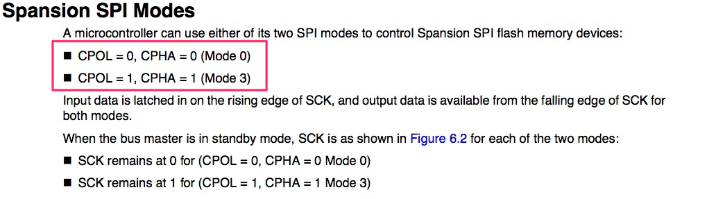
The datasheet explains that the flash IC understands only 2 combinations of
CPOL and CPHA: (CPOL=0, CPHA=0) or (CPOL=1, CPHA=1)
Let’s take a first look at some sniffed data:
In order to understand exactly what’s happenning you’ll need the FL064PIF’s
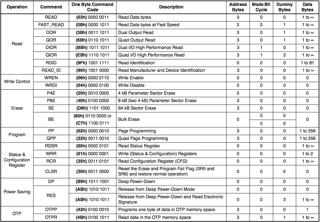
instruction set, available in its datasheet:
Now we can finally analyse the captured data:
In the datasheet we can see that the FL064PIF has high-performance features for
read and write operations: Dual and Quad options that multiplex the data over
more lines to increase the transmission speed. From taking a few samples, it
doesn’t seem like the router uses these features much -if at all-, but it’s
important to keep the possibility in mind in case we see something odd in a
capture.
Transmission modes that require additional pins can be a problem if your logic
analyser is not powerful enough.
The Importance of Your Sampling Rate [Theory]
A logic analyser is a conceptually simple device: It reads signal lines as
digital inputs every x microseconds for y seconds, and when it’s done it
sends the data to your computer to be analysed.
For the protocol analyser to generate accurate data it’s vital that we record
digital inputs faster than the device writes them. Otherwise the data will be
mangled by missing bits or deformed waveforms.
Unfortunately, your logic analyser’s maximum sampling rate depends on how
powerful/expensive it is and how many lines you need to sniff at a time.
High-speed interfaces with multiple data lines can be a problem if you don’t have
access to expensive equipment.
I recorded this data from the Ralink-Flash SPI bus using a low-end Saleae
analyser at its maximum sampling rate for this number of lines,
24 MS/s:
As you can see, even though the clock signal has the 8 low to high transitions
required for each byte, the waveform is deformed.
Since the clock signal is used to coordinate when to read the data lines, this
kind of waveform deformation may cause data corruption even if we don’t drop any
bits (depending partly on the design of your logic analyser). There’s always
some wiggle room for read inaccuracies, and we don’t need 100% correct data at
this point, but it’s important to keep all error vectors in mind.
Let’s sniff the same bus using a higher performance logic analyser at
100 MS/s:
As you can see, this clock signal is perfectly regular when our Sampling Rate is
high enough.
If you see anything dodgy in your traffic capture, consider how much data you’re
willing to lose and whether you’re being limited by your equipment. If that’s
the case, either skip this Reversing vector or consider investing in a better
logic analyser.
Seeing the Data Flow
We’re already familiar with the system thanks to the overview of the firmware
we did in Part 2, so we can think of some specific SPI transmissions that we may
be interested in sniffing. Simply connecting an oscilloscope to the MISO and MOSI
pins will help us figure out how to trigger those transmissions and yield some
other useful data.
Here’s a video (no audio) showing both the serial interface and the MISO/MOSI
signals while we manipulate the router:
This is a great way of easily identifying processes or actions that trigger
flash read/write actions, and will help us find out when to start recording with
the logic analyser and for how long.
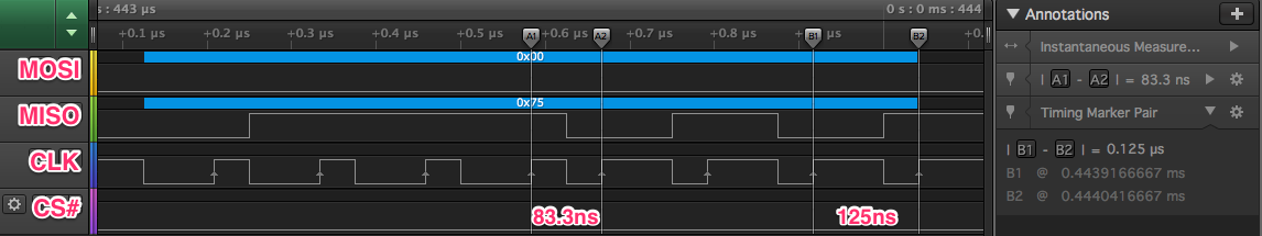
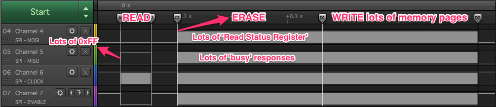
Analysing SPI Traffic - ATP’s Save Command
In Post 2 I mentioned ATP CLI has a save command that stores something to
flash; unfortunately, the help menu (save ?) won’t tell you what it’s doing
and the only output when you run it is a few dots that act as a progress bar.
Why don’t we find out by ourselves? Let’s make a plan:
Wait until boot sequence is complete and the router is idle so there’s no
unexpected SPI traffic
Start the ATP Cli as explained in Part 1
Connect the oscilloscope to MISO/MOSI and run save to get a rough estimate
of how much time we need to capture data for
Set a trigger in the enable line sniffed by the logic analyser so it starts
recording as soon as the flash IC is selected
Run save
Analyse the captured data
Steps 3 and 4 can be combined so you see the data flow in real time in the scope
while you see the charge bar for the logic analyser; that way you can make
sure you don’t miss any data. In order to comfortably connect both scope and
logic sniffer to the same pins, these test clips come in very handy:
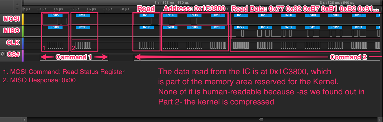
Once we’ve got the traffic we can take a first look at it:
Let’s consider what sort of data could be extracted from this traffic dump that
might be useful to us. We’re working with a memory storage IC, so we can see the
data that is being read/written and the addresses where it belongs. I think we
can represent that data in a useful way by 2 means:
Traffic map depicting which Flash areas are being written, read or erased in
chronological order
Create binary files that replicate the memory blocks that were read/written,
preferably removing all the protocol rubbish that we sniffed along with them.
Saleae’s SPI analyser will export the
data as a CSV file.
Ideally we’d
improve their protocol analyser
to add the functionality we want, but that would be too much work for this
project. One of the great things about low level protocols like SPI is that
they’re usually very straightforward; I decided to write some python spaghetti
code to analyse the CSV file and extract the data we’re looking for:
binmaker.py
and
traffic_mapper.py
The workflow to analyse a capture is the following:
Export sniffed traffic as CSV
Run the script:
Iterate through the CSV file
Identify different commands by their index
Recognise the command expressed by the first byte
Process its arguments (addresses, etc.)
Identify the read/write payload
Convert ASCII representation of each payload byte to binary
Write binary blocks to different files for MISO (read) and MOSI (write)
Read the traffic map (regular text) and the binaries
(hexdump -C output.bin | less)
Replicated Memory Blocks, Split by address:
Files list
The traffic map is much more useful when combined with the Flash memory map we
found in Part 2:
From the traffic map we can see the bulk of the save command’s traffic is
simple:
Read about 64kB of data from the protect area
Overwrite the data we just read
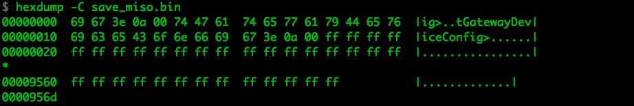
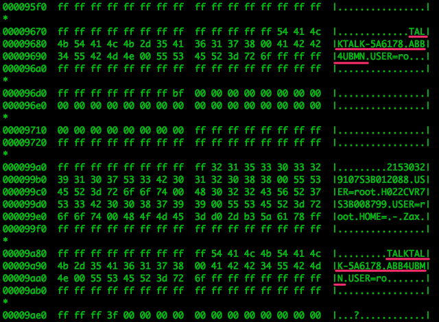
In the MISO binary we can see most of the read data was just tons of 1s:
Most of the data in the MOSI binary is plaintext XML, and it looks exactly like
the /var/curcfg.xml file we discovered in Part 2. As we discussed then, this
“current configuration” file contains tons of useful data, including the current
WiFi credentials.
It’s standard to keep reserved areas in flash; they’re mostly for
miscellaneous data that needs to survive across reboots and be configurable
by user, firmware or factory. It makes sense for a command called save to
write data to such area, it explains why the data is perfectly readable as
opposed to being compressed like the filesystem, and why we found the XML file
in the /var/ folder of the filesystem (it’s a folder for runtime files; data in
the protect area has to be loaded to memory separately from the filesystem).
The Pot of Gold at the End of the Firmware [Theory]
During this whole process it’s useful to have some sort of target to keep you
digging in the same general direction.
Our target is an old one: the algorithm that generates the router’s default WiFi
password. If we get our hands on such algorithm and it happens to derive the
password from public information, any HG533 in the world with default WiFi
credentials would probably be vulnerable.
That exact security issue has been found countless times in the past, usually
deriving the password from public data like the Access Point’s MAC address or
its SSID.
That being said, not all routers are vulnerable, and I personally don’t expect
this one to be. The main reason behind targeting this specific vector is
that it’s caused by a recurrent problem in embedded engineering: The need for
a piece of data that is known by the firmware, unique to each device and known
by an external entity. From default WiFi passwords to device credentials for IoT
devices, this problem manifests in different ways all over the Industry.
Future posts will probably reference the different possibilities I’m about to
explain, so let me get all that theory out of the way now.
The Sticker Problem
In this day and era, connecting to your router via ethernet so there’s no need
for default WiFi credentials is not an option, using a display to show a
randomly generated password would be too expensive, etc. etc. etc.
The most widely adopted solution for routers is to create a WiFi network using
default credentials, print those credentials on a sticker at the factory and
stick it to the back of the device.
The WiFi password is the ‘unique piece of data’, and the computer printing the
stickers in the factory is the ‘external entity’. Both the firmware and the
computer need to know the default WiFi credentials, so the engineer needs to
decide how to coordinate them. Usually there are 2 options available:
The same algorithm is implemented in both the device and the computer, and its
input parameters are known to both of them
A computer generates the credentials for each device and they’re stored
into each device separately
Developer incompetence aside, the first approach is usually taken as a last
resort; if you can’t get your hardware manufacturer to flash unique data to each
device or can’t afford the increase in manufacturing cost.
The second approach is much better by design: We’re not trusting the hardware
with data sensitive enough to compromise every other device in the field. That
being said, the company may still decide to use an algorithm with predictable
outputs instead of completely random data; that would make the system as secure
as the weakest link between the algorithm -mathematically speaking-, the
confidentiality of their source code and the security of the computers/network
running it.
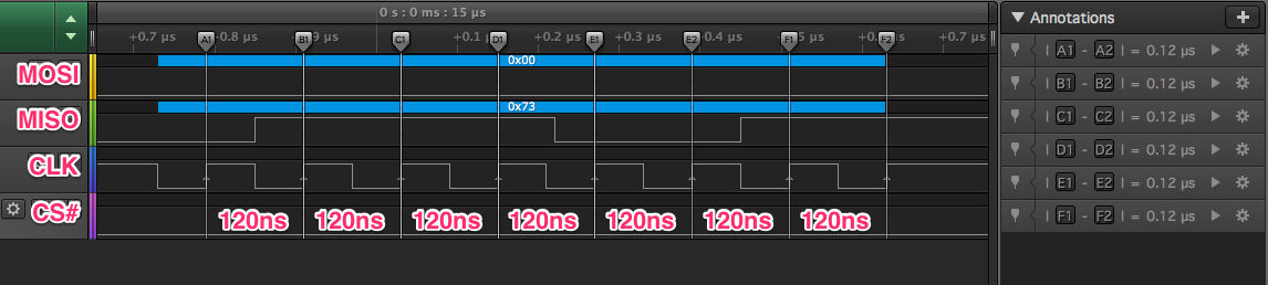
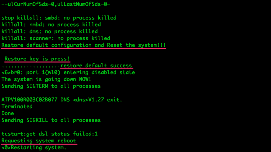
Sniffing Factory Reset
So now that we’ve discussed our target, let’s gather some data about it. The
first thing we wanna figure out is which actions will kickstart the flow of
relevant data on the PCB. In this case there’s 1 particular action: Pressing
the Factory Reset button for 10s. This should replace the existing WiFi
credentials with the default ones, so the default creds will have to be
generated/read. If the key or the generation algorithm need to be retrieved from
Flash, we’ll see them in a traffic capture.
That’s exactly what we’re gonna do, and we’re gonna observe the UART interface,
the oscilloscope and the logic analyser during/after pressing the reset button.
The same process we followed for ATP’s save gives us these results:
The traffic map tells us the device first reads and overwrites 2 large chunks
of data from the protect area and then reads a smaller chunk of data from the
filesystem (possibly part of the next process to execute):
Once again, we combine transmission map and binary files to gain some insight
into the system. In this case, the ‘factory reset’ code seems to:
Read ATP_LOG from Flash; it contains info such as remote router accesses or
factory resets. It ends with a large chunk of 1s (0xff)
Overwrite that memory segment with 1s
write a ‘new’ ATP_LOG followed by the “current configuration” curcfg.xml
file
Read compressed (unintelligible to us) memory chunk from the filesystem
The chunk from the filesystem is read AFTER writing the new password to Flash,
which doesn’t make sense for a password generation algorithm. That being said,
the algorithm may be already loaded into memory, so its absence in the SPI
traffic is not conclusive on whether or not it exists.
As part of the MOSI data we can see the new WiFi password be saved to Flash
inside the XML string:
What about the default password being read? If we look in the MISO binary, it’s
nowhere to be seen. Either the Ralink is reading it using a different mode
(secure/dual/quad/?) or the credentials/algorithm are already loaded in RAM (no
need to read them from Flash again, since they can’t change). The later seems
more likely, so I’m not gonna bother updating my scripts to support different
read modes. We write down what we’ve found and we’ll get back to the default
credentials in the next part.
Since we’re at it, let’s take a look at the SPI traffic generated when setting
new WiFi credentials via HTTP:
Map,
MISO,
MOSI.
We can actually see the default credentials being read from the protect area
of Flash this time (not sure why the Ralink would load it to set a new
password; it’s probably incidental):
As you can see, they’re in plain text and separated from almost anything else
in Flash. This may very well mean there’s no password generation algorithm in
this device, but it is NOT conclusive. The developers could have decided to
generate the credentials only once (first boot?) and store them to flash in order
to limit the number of times the algorithm is accessed/executed, which helps hide
the binary that contains it. Otherwise we could just observe the running
processes in the router while we press the Factory Reset button and see which
ones spawn or start consuming more resources.
Next Steps
Now that we’ve got the code we need to create binary recreations of the traffic
and transmission maps, getting from a capture to binary files takes seconds. I
captured other transmissions such as the first few seconds of boot
(map,
miso),
but there wasn’t much worth discussing.
The ability to easily obtain such useful data will probably come in handy moving
forward, though.
In the next post we get the data straight from the source, communicating with
the Flash IC directly to dump its memory. We’ll deal with compression algorithms
for the extracted data, and we’ll keep piecing everything together.
In part 1 we found a debug UART port that gave us access to a Linux shell. At
this point we’ve got the same access to the router that a developer would use to
debug issues, control the system, etc.
This first overview of the system is easy to access, doesn’t require expensive
tools and will often yield very interesting results. If you want to
do some hardware hacking but don’t have the time to get your hands too dirty,
this is often the point where you stop digging into the hardware and start
working on the higher level interfaces: network vulnerabilities, ISP
configuration protocols, etc.
These posts are hardware-oriented, so we’re just gonna use this access to gather
some random pieces of data. Anything that can help us understand the system or
may come in handy later on.
Please check out the
legal disclaimer
in case I come across anything sensitive.
Full disclosure: I’m in contact with Huawei’s security team; they’ve had time
to review the data I’m going to reveal in this post and confirm there’s nothing
too sensitive for publication. I tried to contact TalkTalk, but their security
staff is nowhere to be seen.
Picking Up Where We Left Off
We get our serial terminal application up and running in the computer and power
up the router.
We press enter and get the login prompt from ATP Cli; introduce the
credentials admin:admin and we’re in the ATP command line. Execute the command
shell and we get to the BusyBox CLI (more on BusyBox later).
-------------------------------
-----Welcome to ATP Cli------
-------------------------------
Login: admin
Password:    #Password is ‘admin'
ATP>shell
BusyBox vv1.9.1 (2013-08-29 11:15:00 CST) built-in shell (ash)
Enter 'help' for a list of built-in commands.
# ls
var   usr   tmp   sbin  proc  mnt   lib   init  etc   dev   bin
At this point we’ve seen the 3 basic layers of firmware in the Ralink IC:
U-boot: The device’s bootloader. It understands the device’s memory map,
kickstarts the main firmware execution and takes care of some other low level
tasks
Linux: The router is running Linux to keep overall control of the hardware,
coordinate parallel processes, etc. Both ATP CLI and BusyBox run on top of it
Busybox: A small binary including reduced versions of multiple linux
commands. It also supplies the shell we call those commands from.
Lower level interfaces are less intuitive, may not have access to all the data
and increase the chances of bricking the device; it’s always a good idea to
start from BusyBox and walk your way down.
For now, let’s focus on the boot sequence itself. The developers thought it would
be useful to display certain pieces of data during boot, so let’s see if there’s
anything we can use.
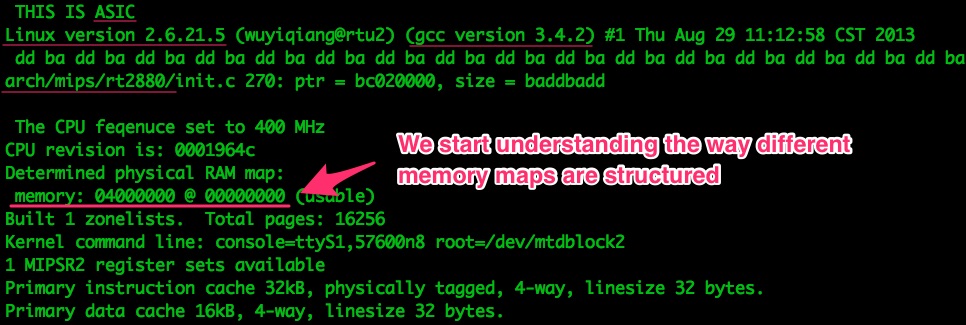
Boot Debug Messages
We find multiple random pieces of data scattered across the boot sequence. We’ll
find useful info such as the compression algorithm used for some flash segments:
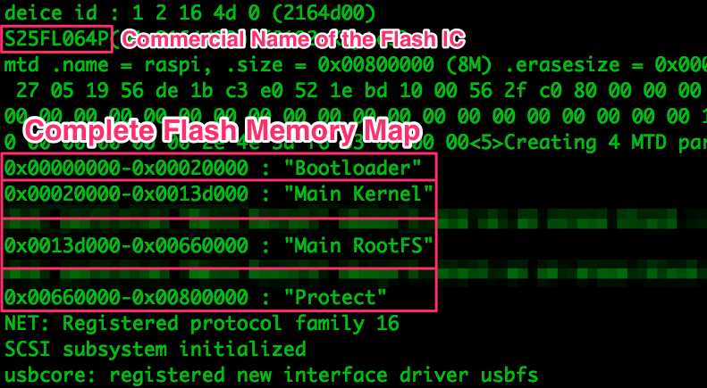
Intel on how the external flash memory is structured will be very useful when we
get to extracting it.
And more compression intel:
We’ll have to deal with the compression algorithms when we try to access the raw
data from the external Flash, so it’s good to know which ones are being used.
What Are ATP CLI and BusyBox Exactly? [Theory]
The Ralink IC in this router runs a Linux kernel to control memory and parallel
processes, keep overall control of the system, etc. In this case, according to
the Ralink’s
product brief,
they used the Linux 2.6.21 SDK. ATP CLI is a CLI running either on top of
Linux or as part of the kernel. It provides a first layer of authentication into
the system, but other than that it’s very limited:
ATP>help
Welcome to ATP command line tool.
If any question, please input "?" at the end of command.
ATP>?
cls
debug
help
save
?
exit
ATP>
help doesn’t mention the shell command, but it’s usually either shell or
sh. This ATP CLI includes less than 10 commands, and doesn’t support any kind
of complex process control or file navigation. That’s where BusyBox comes in.
BusyBox is a single binary containing reduced versions of common unix
commands, both for development convenience and -most importantly- to save memory.
From ls and cd to top, System V init scripts and pipes, it allows us to
use the Ralink IC somewhat like your regular Linux box.
One of the utilities the BusyBox binary includes is the shell itself, which has
access to the rest of the commands:
ATP>shell
BusyBox vv1.9.1 (2013-08-29 11:15:00 CST) built-in shell (ash)
Enter 'help' for a list of built-in commands.
# ls
var   usr   tmp   sbin  proc  mnt   lib   init  etc   dev   bin
#
# ls /bin
zebra        swapdev      printserver  ln           ebtables     cat
wpsd         startbsp     pppc         klog         dns          busybox
wlancmd      sntp         ping         kill         dms          brctl
web          smbpasswd    ntfs-3g      iwpriv       dhcps        atserver
usbserver    smbd         nmbd         iwconfig     dhcpc        atmcmd
usbmount     sleep        netstat      iptables     ddnsc        atcmd
upnp         siproxd      mount        ipp          date         at
upg          sh           mldproxy     ipcheck      cwmp         ash
umount       scanner      mknod        ip           cp           adslcmd
tr111        rm           mkdir        igmpproxy    console      acl
tr064        ripd         mii_mgr      hw_nat       cms          ac
telnetd      reg          mic          ethcmd       cli
tc           radvdump     ls           equipcmd     chown
switch       ps           log          echo         chmod
#
You’ll notice different BusyBox quirks while exploring the filesystem, such
as the symlinks to a busybox binary in
/bin/.
That’s good to know, since any commands that may contain sensitive data will
not be part of the BusyBox binary.
Exploring the File System
Now that we’re in the system and know which commands are available, let’s see if
there’s anything useful in there. We just want a first overview of the system,
so I’m not gonna bother exposing every tiny piece of data.
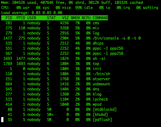
The top command will help us identify which processes are consuming the most
resources. This can be an extremely good indicator of whether some processes are
important or not. It doesn’t say much while the router’s idle, though:
One of the processes running is usbmount, so the router must support connecting
‘something’ to the USB port. Let’s plug in a flash drive in there…
usb 1-1: new high speed USB device using rt3xxx-ehci and address 2
[...]
++++++sambacms.c 2374 renice=renice -n +10 -p 1423
The USB is recognised and mounted to /mnt/usb1_1/, and a samba server is
started. These files show up in /etc/samba/:
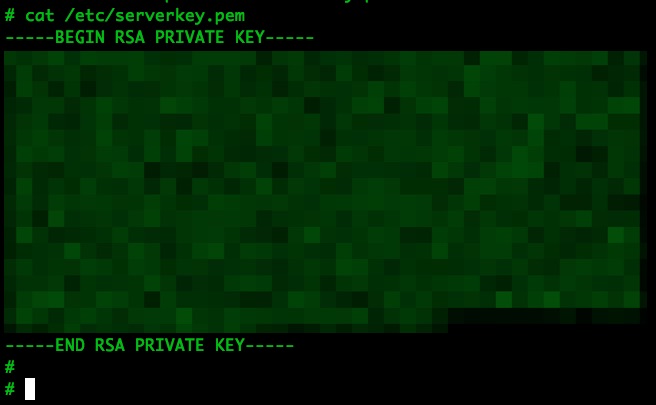
/var/ and /etc/ always contain tons of useful data, and some of it makes
itself obvious at first sight. Does that say /etc/serverkey.pem??
¯\_(ツ)_/¯
It’s common to find private keys in embedded systems. They could be RSA private
keys used for mutually-authenticated TLS connections with a server, variables
buried in a file to be loaded by an application, etc. By accessing 1 single
device via hardware you may obtain the keys that will help you eavesdrop
encrypted connections, attack servers, end users or other devices in the fleet.
This key could be used to communicate with some server from Huawei or the ISP,
although that’s less common. On the other hand, it’s also very common to find
public certs used to communicate with remote servers.
In this case we find 2 certificates next to the private key; both are self-signed
by the same ‘person’:
/etc/servercert.pem: Most likely the certificate for the serverkey
/etc/root.pem:
Probably used to connect to a server from the ISP or Huawei. Not sure.
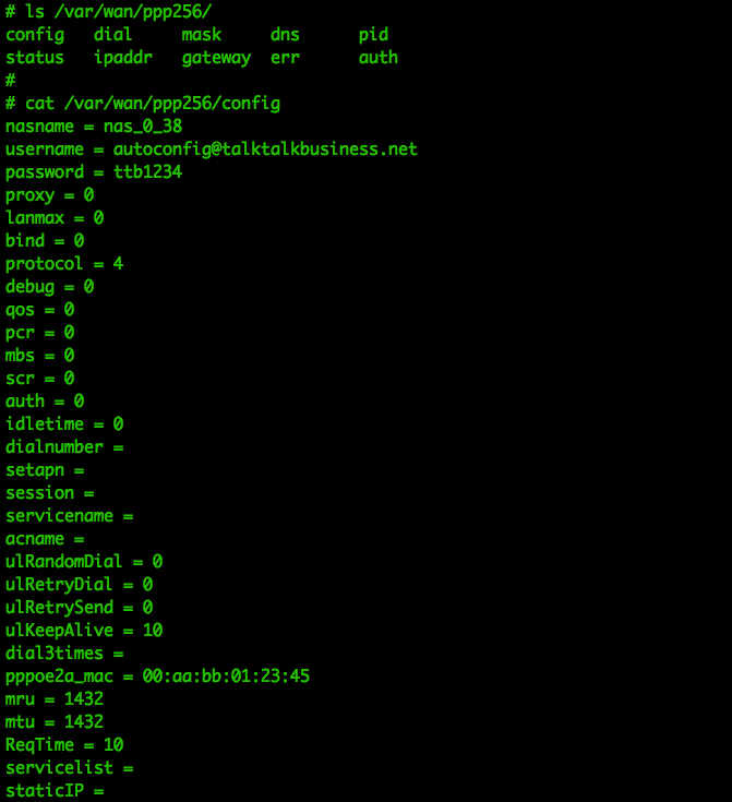
And some more data in /etc/ppp256/config and /etc/ppp258/config:
These credentials are also available via the HTTP interface, which is why I’m
publishing them, but that’s not the case in many other routers (more on this
later).
With so many different files everywhere it can be quite time consuming to go
through all the info without the right tools. We’re gonna copy as much data as
we can into the USB drive and go through it on our computer.
The Rambo Approach to Intel Gathering
Once we have as many files as possible in our computer we can check some things
very quick. find . -name *.pem reveals there aren’t any other TLS certificates.
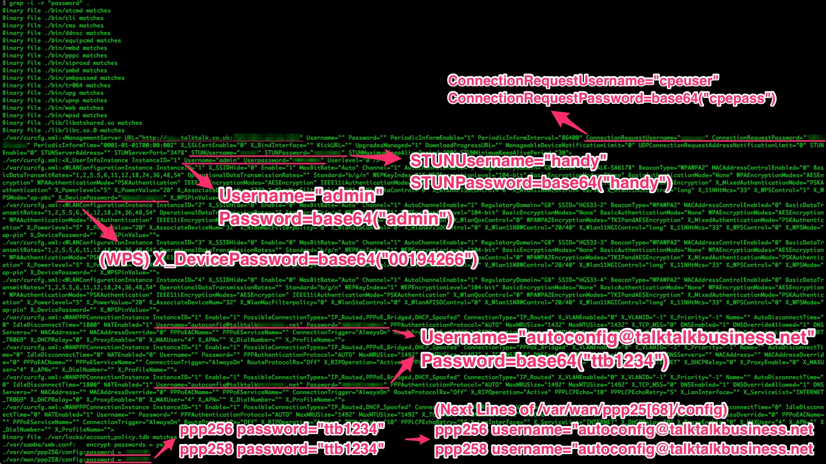
What about searching the word password in all files? grep -i -r password .
We can see lots of credentials; most of them are for STUN, TR-069 and local
services. I’m publishing them because this router proudly displays
them all via the HTTP interface, but those are usually hidden.
If you wanna know what happens when someone starts pulling from that thread,
check out Alexander Graf’s talk
“Beyond Your Cable Modem”,
from CCC 2015. There are many other talks about attacking TR-069 from DefCon,
BlackHat, etc. etc.
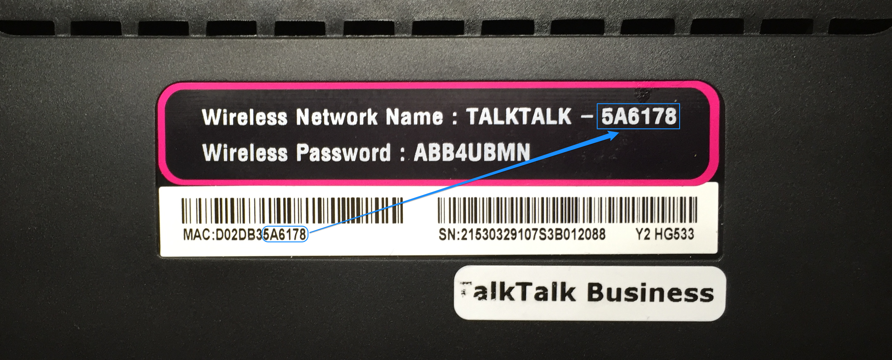
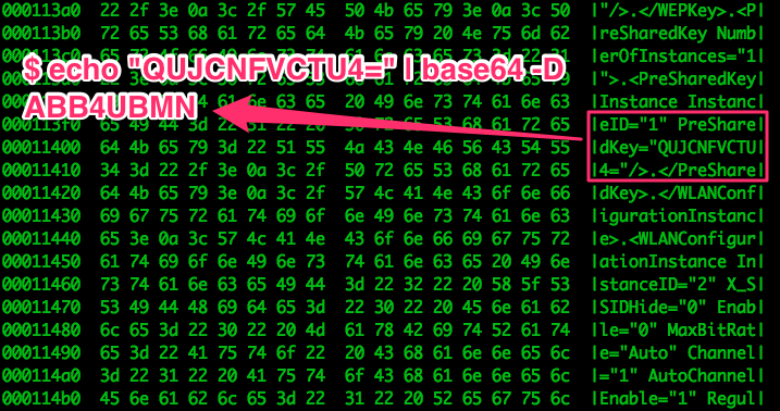
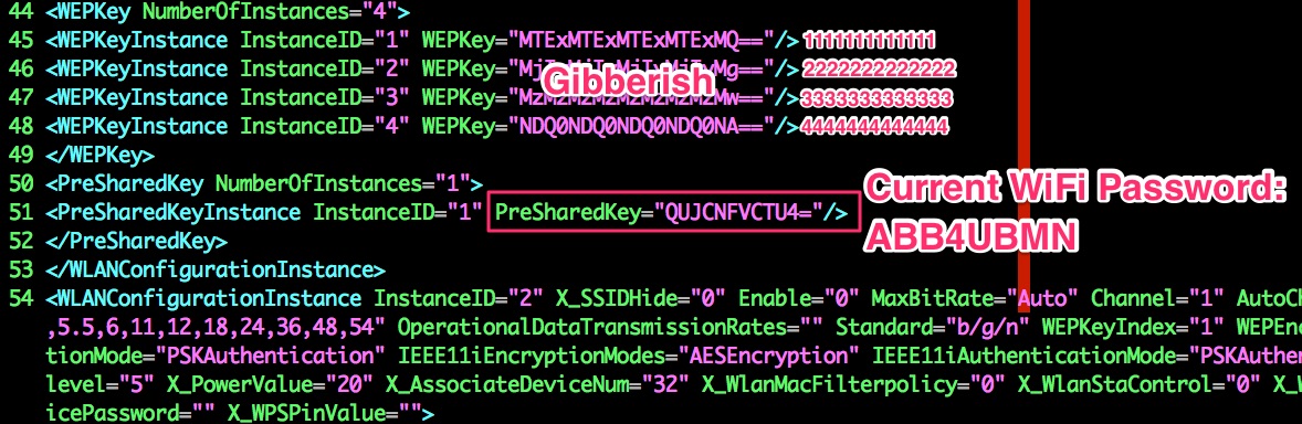
The credentials we can see are either in plain text or encoded in base64.
Of course, encoding is worthless for data protection:
$ echo "QUJCNFVCTU4=" | base64 -D
ABB4UBMN
That is the current WiFi password set in the router. It leads us to 2 VERY
interesting files. Not just because of their content, but because they’re a
vital part of how the router operates:
/var/curcfg.xml:
Current configuration file. Among other things, it contains the current WiFi
password encoded in base64
/etc/defaultcfg.xml:
Default configuration file, used for ‘factory reset’. Does not include the
default WiFi password (more on this in the next posts)
Exploring ATP’s CLI
The ATP CLI includes very few commands. The most interesting one -besides
shell- is
debug.
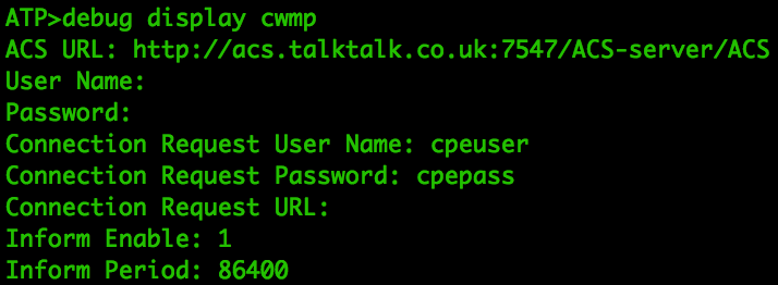
This isn’t your regular debugger; debug display will simply give you some info
about the commands igmpproxy, cwmp, sysuptime or atpversion.
Most of them
don’t have anything juicy, but what about cwmp? Wasn’t that related to remote
configuration of routers?
Once again, these are the CWMP (TR-069) credentials used for remote router
configuration. Not even encoded this time.
The rest of the ATP commands are pretty useless: clear screen, help menu, save
to flash and exit. Nothing worth going into.
Exploring Uboot’s CLI
The bootloader’s command line interface offers raw access to some memory areas.
Unfortunately, it doesn’t give us direct access to the Flash IC, but let’s
check it out anyway.
Please choose operation:
   3: Boot system code via Flash (default).
   4: Entr boot command line interface.
You choosed 4
Stopped Uboot WatchDog Timer.
4: System Enter Boot Command Line Interface.
U-Boot 1.1.3 (Aug 29 2013 - 11:16:19)
RT3352 # help
?       - alias for 'help'
bootm   - boot application image from memory
cp      - memory copy
erase   - erase SPI FLASH memory
go      - start application at address 'addr'
help    - print online help
md      - memory display
mdio   - Ralink PHY register R/W command !!
mm      - memory modify (auto-incrementing)
mw      - memory write (fill)
nm      - memory modify (constant address)
printenv- print environment variables
reset   - Perform RESET of the CPU
rf      - read/write rf register
saveenv - save environment variables to persistent storage
setenv  - set environment variables
uip - uip command
version - print monitor version
RT3352 #
Don’t touch commands like erase, mm, mw or nm unless you know exactly
what you’re doing; you’d probably just force a router reboot, but in some cases
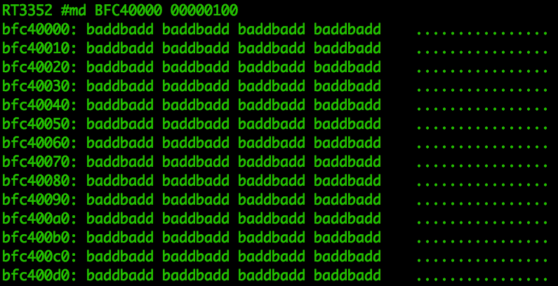
you may brick the device. In this case, md (memory display) and printenv
are the commands that call my atention.
We can see settings like the UART baudrate, as well as some interesting memory
locations. Those memory addresses are not for the Flash IC, though. The flash
memory is only addressed by 3 bytes: [0x00000000, 0x00FFFFFF].
Let’s take a look at some of them anyway, just to see the kind of access this
interface offers.What about kernel_addr=BFC40000?
Nope, that badd message means bad address, and it has been hardcoded in md
to let you know that you’re trying to access invalid memory locations. These
are good addresses, but they’re not accessible to u-boot at this point.
It’s worth noting that by starting Uboot’s CLI we have stopped the router from
loading the linux Kernel onto memory, so this interface gives access to a very
limited subset of data.
We can find random pieces of data around memory using this method (such as that
SPI Flash Image string), but it’s pretty hopeless for finding anything specific.
You can use it to get familiarised with the memory architecture, but that’s about
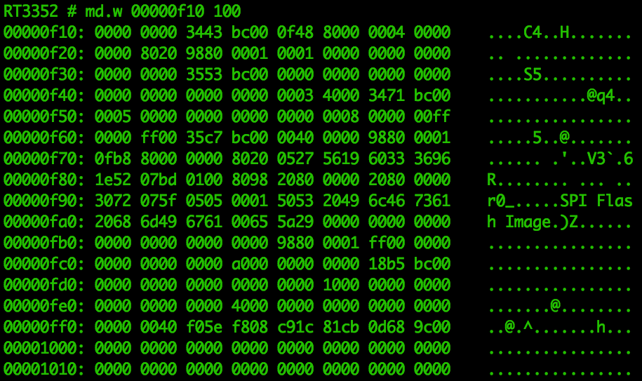
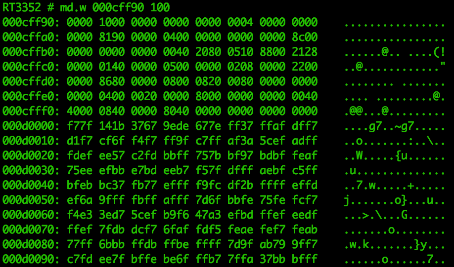
it. For example, there’s a very obvious change in memory contents at
0x000d0000:
And just because it’s about as close as it gets to seeing the girl in the red
dress, here is the md command in action. You’ll notice it’s very easy to spot
that change in memory contents at 0x000d0000.
Next Steps
In the next post we combine firmware and bare metal, explain how data flows
and is stored around the device, and start trying to manipulate the system to
leak pieces of data we’re interested in.
In this series of posts we’re gonna go through the process of Reverse Engineering
a router. More specifically, a Huawei HG533.
At the earliest stages, this is the most basic kind of reverse engineering.
We’re simple looking for a serial port that the engineers who designed the device
left in the board for debug and -potentially- technical support purposes.
Even though I’ll be explaining the process using a router, it can be applied to
tons of household embedded systems. From printers to IP cameras, if
it’s mildly complex it’s quite likely to be running some form of linux. It will
also probably have hidden debug ports like the ones we’re gonna be looking for
in this post.
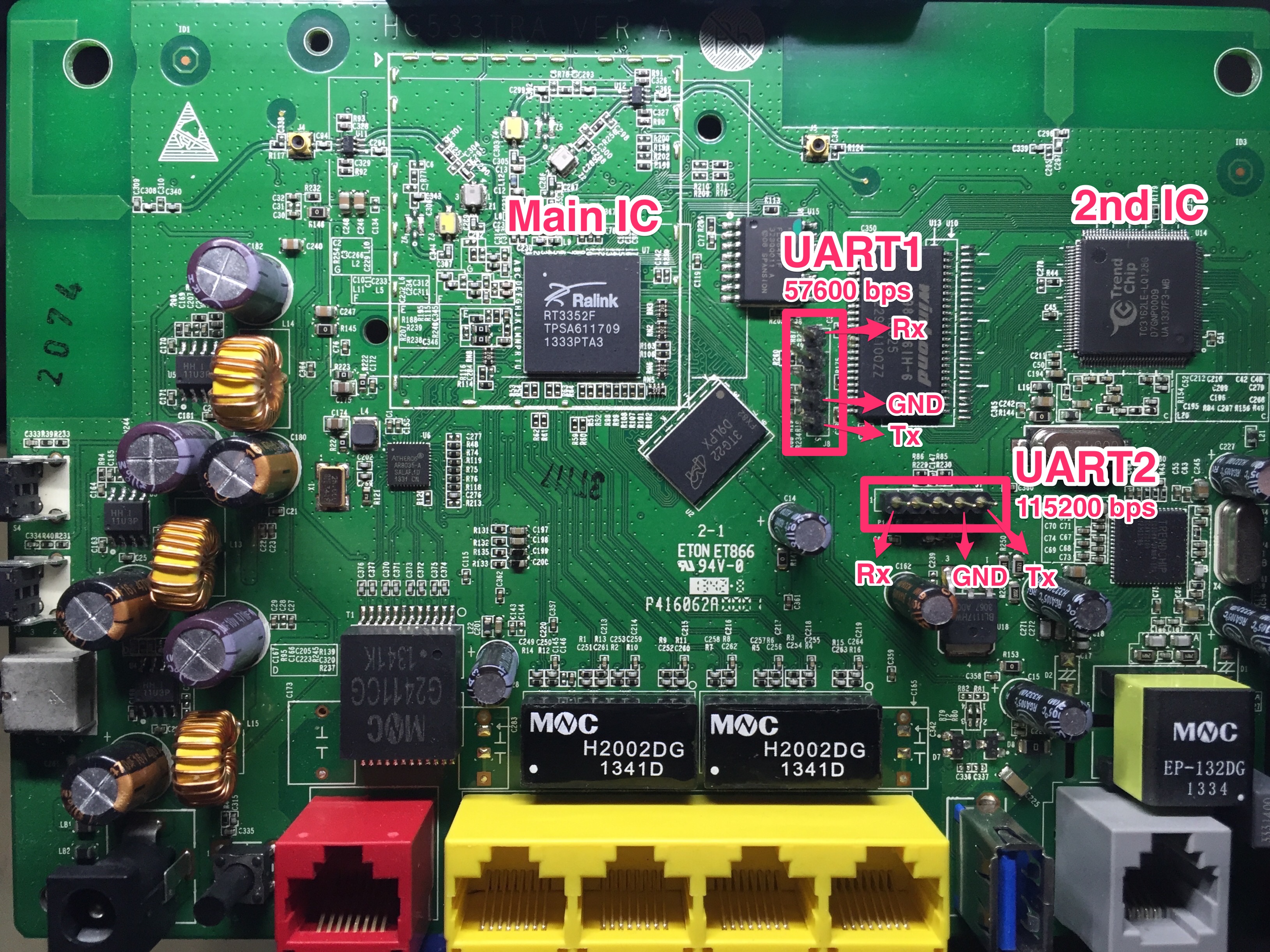
Finding the Serial Port
Most UART ports I’ve found in commercial products are between 4 and 6 pins,
usually neatly aligned and sometimes marked in the PCB’s silkscreen somehow.
They’re not for end users, so they almost never have pins or connectors attached.
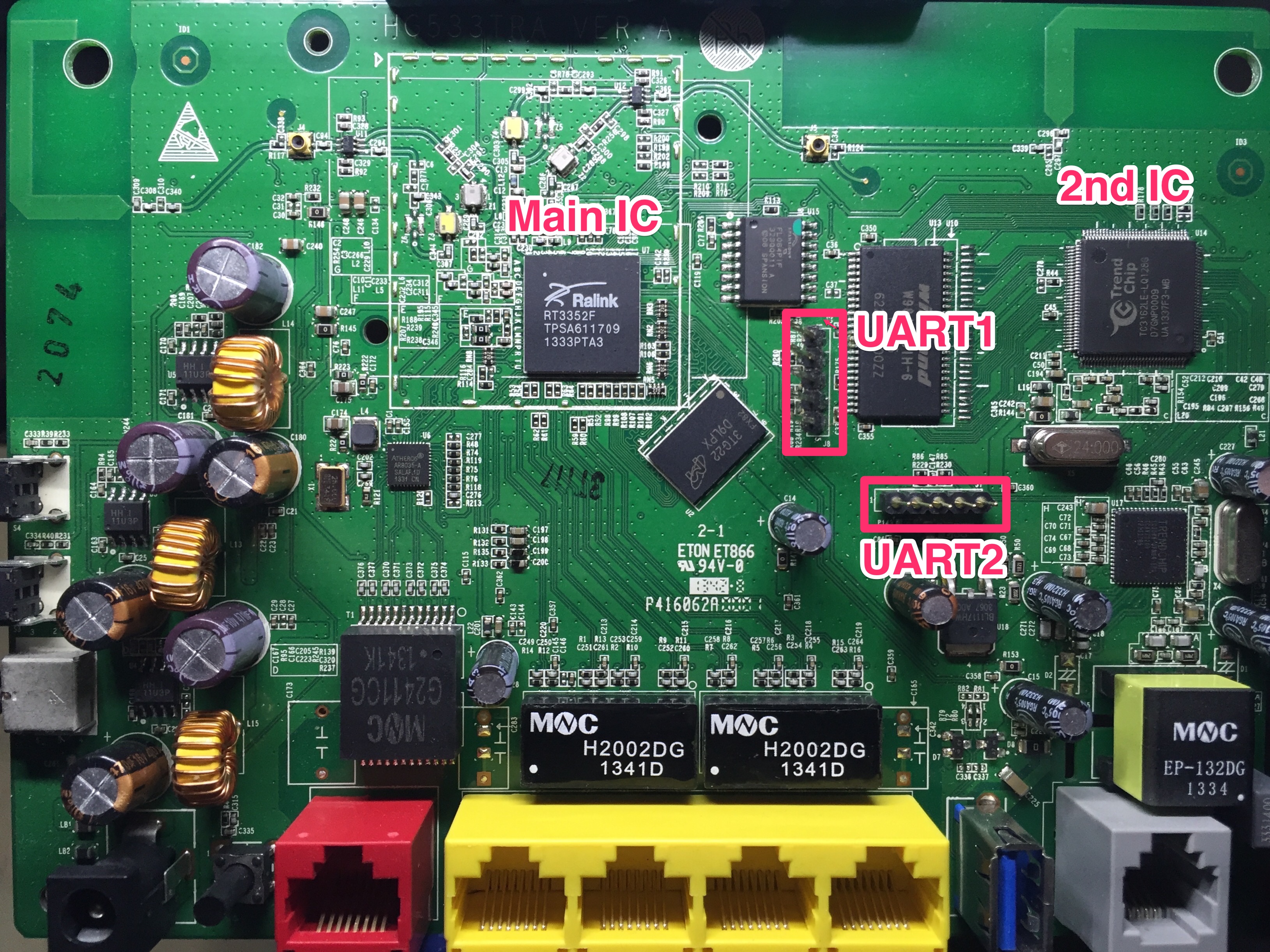
After taking a quick look at the board, 2 sets of unused pads call my atention
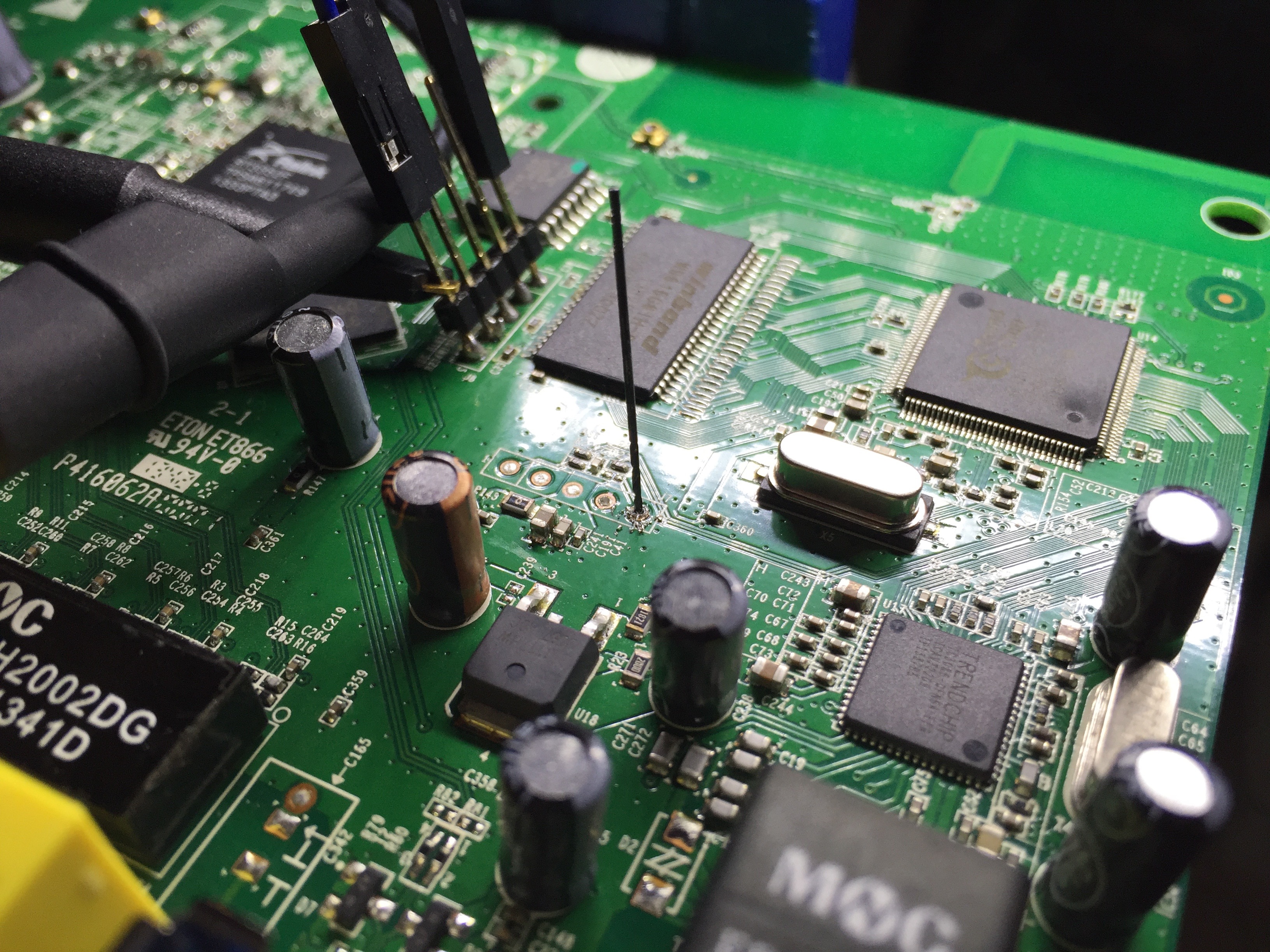
(they were unused before I soldered those pins in the picture, anyway):
This device seems to have 2 different serial ports to communicate with
2 different Integrated Circuits (ICs). Based on the location on the board and
following their traces we can figure out which one is connected to the main IC.
That’s the most likely one to have juicy data.
In this case we’re simply gonna try connecting to both of them and find out what
each of them has to offer.
Identifying Useless Pins
So we’ve found 2 rows of pins that -at first sight- could be UART ports. The
first thing you wanna do is find out if any of those contacts is useless.
There’s a very simple trick I use to help find useless pads:
Flash a bright light from the backside of the PCB and look at it from directly
above. This is what that looks like:
We can see if any of the layers of the PCB is making contact with the solder
blob in the middle of the pad.
Connected to something (we can see a trace “at 2 o’clock”)
NOT CONNECTED
100% connected to a plane or thick trace. It’s almost certainly a power pin,
either GND or Vcc
Connections at all sides. This one is very likely to be the other power pin.
There’s no reason for a data pin in a debug port to be connected to 4 different
traces, but the pad being surrounded by a plane would explain those connections
Connected to something
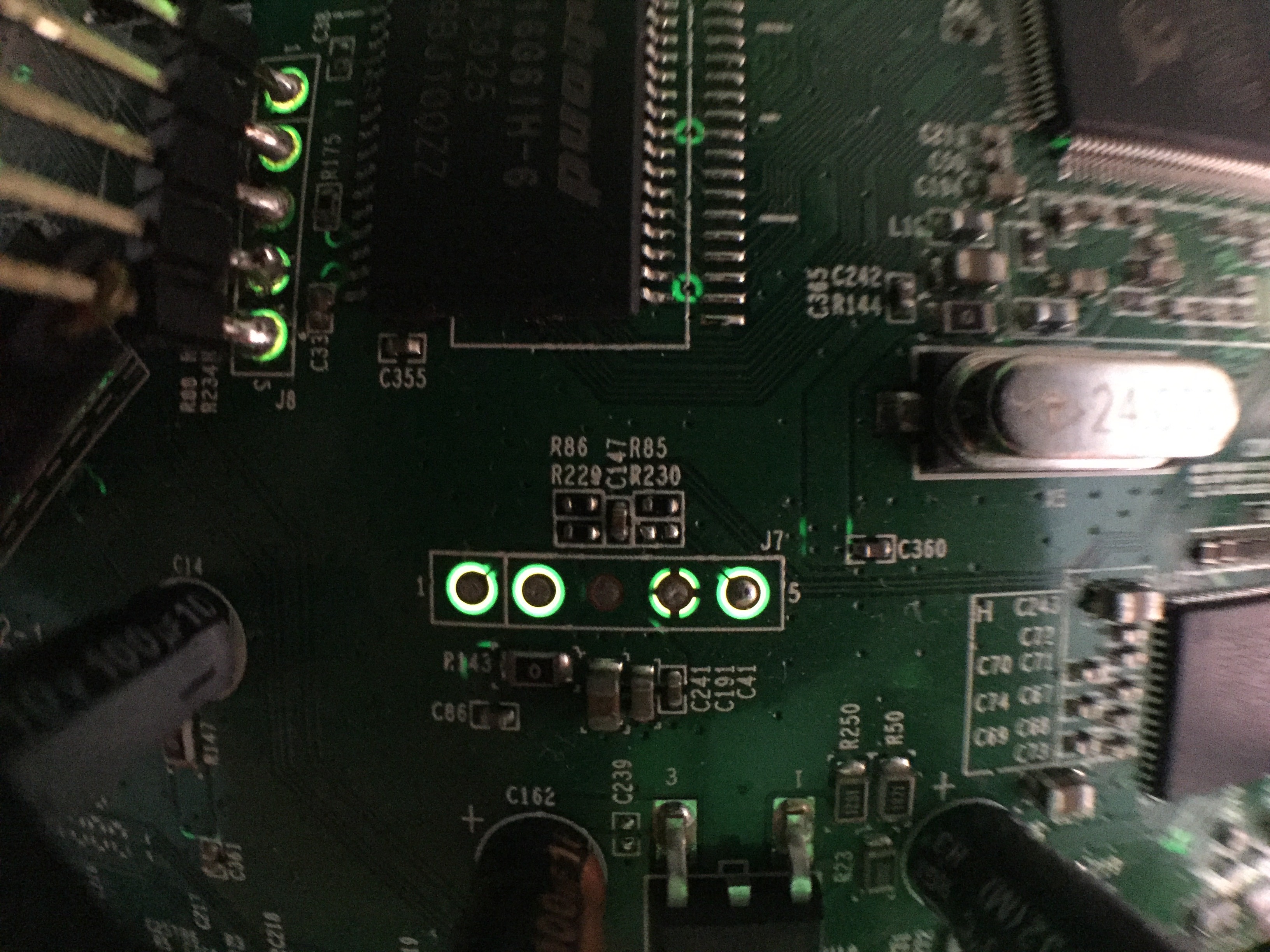
Soldering Pins for Easy Access to the Lines
In the picture above we can see both serial ports.
The pads in these ports are through-hole, but the holes themselves are filled in
with blobs of very hard, very high melting point solder.
I tried soldering the pins over the pads, but the solder they used is not easy
to work with. For the 2nd serial port I decided to drill through the solder blobs
with a Dremel and a needle bit. That way we can pass the pins through the holes
and solder them properly on the back of the PCB. It worked like a charm.
Identifying the Pinout
So we’ve got 2 connectors with only 3 useful pins each. We still haven’t verified
the ports are operative or identified the serial protocol used by the device, but
the number and arrangement of pins hint at UART.
Let’s review the UART protocol. There are 6 pin types in the spec:
Tx [Transmitting Pin. Connects to our Rx]
Rx [Receiving Pin. Connects to our Tx]
GND [Ground. Connects to our GND]
Vcc [The board’s power line. Usually 3.3V or 5V. DO NOT CONNECT]
CTS [Typically unused]
DTR [Typically unused]
We also know that according to the Standard, Tx and Rx are pulled up (set to 1)
by default. The Transmitter of the line (Tx) is in charge of pulling it up,
which means if it’s not connected the line’s voltage will float.
So let’s compile what we know and get to some conclusions:
Only 3 pins in each header are likely to be connected to anything. Those
must be Tx, Rx and GND
Two pins look a lot like Vcc and GND
One of them -Tx- will be pulled up by default and be transmitting data
The 3rd of them, Rx, will be floating until we connect the other end of the
line
That information seems enough to start trying different combinations with your
UART-to-USB bridge, but randomly connecting pins you don’t understand is how you
end up blowing shit up.
Let’s keep digging.
A multimeter or a logic analyser would be enough to figure out which pin is
which, but if you want to understand what exactly is going on in each pin,
nothing beats a half decent oscilloscope:
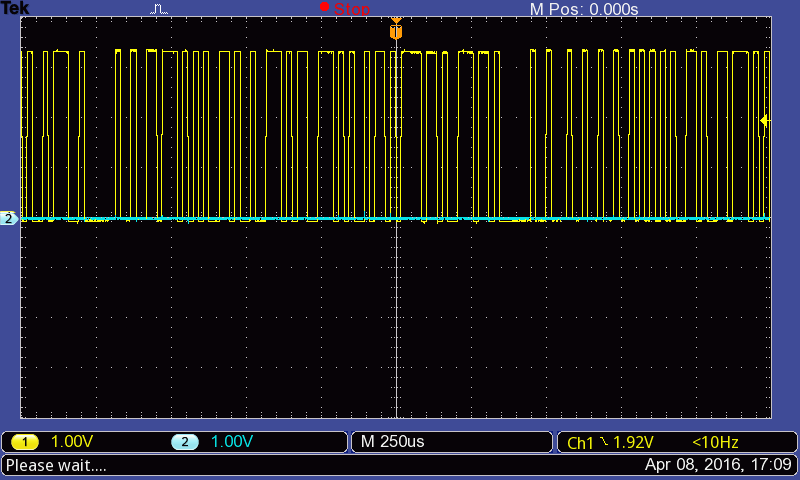
After checking the pins out with an oscilloscope, this is what we can see in
each of them:
GND and Vcc verified - solid 3.3V and 0V in pins 2 and 3, as expected
Tx verified - You can clearly see the device is sending information
One of the pins floats at near-0V. This must be the device’s Rx, which is
floating because we haven’t connected the other side yet.
So now we know which pin is which, but if we want to talk to the serial port
we need to figure out its baudrate. We can find this with a simple
protocol dump from a logic analyser. If you don’t have one, you’ll have to play
“guess the baudrate” with a list of the most common ones until you get readable
text through the serial port.
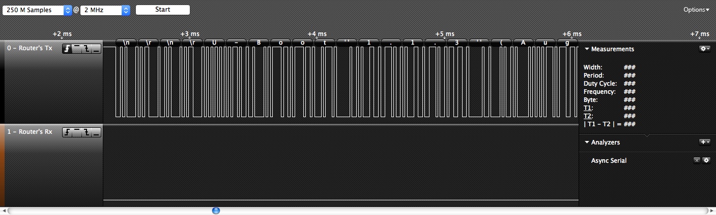
This is a dump from a logic analyser in which we’ve enabled protocol analysis
and tried a few different baudrates. When we hit the right one, we start seeing
readable text in the sniffed serial data (\n\r\n\rU-Boot 1.1.3 (Aug...)
Once we have both the pinout and baudrate, we’re ready to start communicating
with the device:
Connecting to the Serial Ports
Now that we’ve got all the info we need on the hardware side, it’s time to start
talking to the device. Connect any UART to USB bridge you have around and start
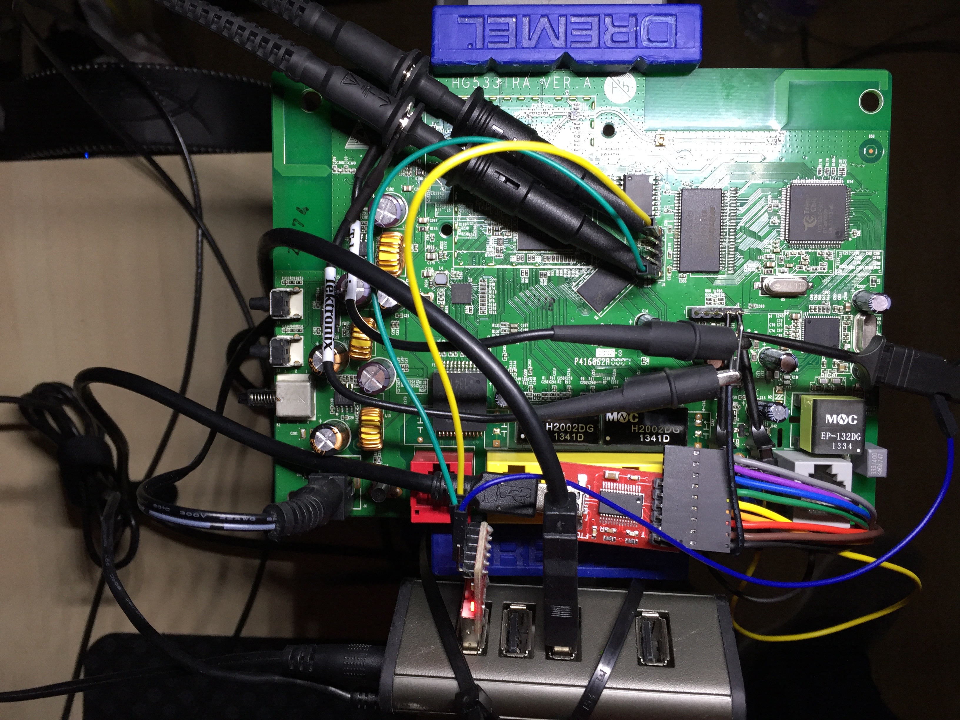
wandering around. This is my hardware setup to communicate with both serial
ports at the same time and monitor one of the ports with an oscilloscope:
And when we open a serial terminal in our computer to communicate with the device,
the primary UART starts spitting out useful info. These are the commands I use
to connect to each port as well as the first lines they send during the boot
process:
Please choose operation:
   3: Boot system code via Flash (default).
   4: Entr boot command line interface.
 0
‘Command line interface’?? We’ve found our way into the system! When we press 4
we get a command line interface to interact with the device’s bootloader.
Furthermore, if we let the device start as the default 3, wait for it to
finish booting up and press enter, we get the message Welcome to ATP Cli
and a login prompt. If the devs had modified the password this step would be a
bit of an issue, but it’s very common to find default credentials in embedded
systems. After a few manual tries, the credentials admin:admin succeeded and I
got access into the CLI:
-------------------------------
-----Welcome to ATP Cli------
-------------------------------

Login: admin
Password:    #Password is ‘admin'
ATP>shell

BusyBox vv1.9.1 (2013-08-29 11:15:00 CST) built-in shell (ash)
Enter 'help' for a list of built-in commands.

# ls
var   usr   tmp   sbin  proc  mnt   lib   init  etc   dev   bin
Running the shell command in ATP will take us directly into Linux’s CLI with
root privileges :)
This router runs BusyBox, a linux-ish interface which I’ll talk about in more
detail in the next post.
Next Steps
Now that we have access to the BusyBox CLI we can start nosing around the software.
Depending on what device you’re reversing there could be plain text passwords,
TLS certificates, useful algorithms, unsecured private APIs, etc. etc. etc.
In the next post we’ll focus on the software side of things. I’ll explain the
differences between boot modes, how to dump memory, and other fun things
you can do now that you’ve got direct access to the device’s firmware.
Some time ago I recorded a slow motion clip of myself picking a cut-away lock.
This kind of lock is used for lock picking practice, as it lets you see the pins
and springs that make the lock work.
In this clip we can see the racking method. Racking a lock is the Rambo approach
to non-destructive lock picking: You jam a racking pick into the lock (half
diamond, snowman, saw… Pretty much any pick but a hook) and move it around;
you play with the force applied in the tension wrench until all the pins lock in
place.
This technique works beautifully here because we don’t have any security pins
in the lock. Security pins usually require a more precise approach and need to
be carefully picked pin by pin.
Slow motion
Regular speed
This is the same video at real time speed. As you can see, the whole process is
pretty quick.
Explaining the video
Too much pressure in the tension wrench caused the first pin to overset (the lower
part of the first pin got stuck between the cilinder -the piece that turns when
the lock is opened- and the case).
After reducing the force applied in the wrench we can see the pin drop and lock
into position. The lock is now ready to be opened.