After having recently purchased a home, I’ve been working on setting up some
level of smart home automation/connectivity.
One of the things in my list was the ability to control my air conditioning
remotely using my phone, so I can get it running before I get home, have it turn
off when I leave, etc.
But how?
System Overview
There are 3 components in my very old Mitsubishi Electric HVAC system:
Indoor (Main) Unit: This is the unit that is inside the house. In my case,
hidden over the drop ceiling in the bathroom. It conditions the air (cooling
or heating), blows it through the ducts, controls its humidity, filters it…
But most importantly for our purposes, it holds the control board that manages
the overall system.
Outdoor Unit: It compresses the refrigerant, and is responsible for the heat
exchange with the outside air.
Remote Controller: This is the wall-mounted device that allows you to configure
the system. It has a display and buttons
For all the technical details, you can refer to your system’s manual. In my case,
the Technical & Service Manual
proved very useful.
And when it homes to my smart home setup, I mostly use Zigbee devices, along
with some Matter devices. Apple HomePod Minis manage the Matter network, while
a Raspberry Pi running Home Assistant is used as the Zigbee hub. Home Assistant
also acts as a bridge between the two networks.
Zigbee is a low-power, low-bandwidth, mesh network protocol that is widely used
in smart home devices. It is highly flexible, powerful and widely adopted.
Matter is a new protocol that aims to unify the smart home ecosystem, and is
backed by Apple, Google, Amazon, and others. It is based on the Thread protocol,
which is a mesh network protocol that is highly efficient and secure. The
downside of its interoperatbility is that it impacts the flexibility of the
protocol, as it defines a series of standard device profiles/types, and devices
are expected some degree of compliance with these profiles.
Approach 1: Buy an off-the-shelf solution
The first approach I considered was to just buy a smart HVAC controller that
would grant me full control over the system: Setting temperatures, fan speeds,
modes, etc.
These sometimes connect to IR/RF interfaces in the remote controller, or more
commonly, they connect to the indoor unit’s control board directly. In the case
of Mitsubishi Electric systems, there are commercial solutions that connect to
the CN105 port in the controal board, granting you full access to the system.
These solutions are optimal, but in my case they were not viable. My unit is
too old and does not have a CN105 port or IR/RF interfaces to connect to. If I
want to connect this thing without replacing very significant parts of the
system, I need to go DIY.
Approach 2: Reverse engineer the communications between the remote controller and the indoor unit
The remote controller is connected to the indoor unit using a 2-wire cable. it
provides power to the remote controller over those 2 lines, and also carries
the bidirectional communication between the two devices.
It might grant me full control over the system, but I just don’t have enough free
time nowadays to dive into this rabbit hole. I also don’t need that level of
control, since I very rarely change the settings in the system. I just need to
turn it on and off.
Approach 3: Create an Arduino Nano Matter implant for the remote controller
Earlier this year, Arduino released a new board called the
Arduino Nano Matter. It was built
in collaboration with Silicon Labs, the creators of the Matter-enabled chip
that it is based on, the MGM240S.
In order to avoid the complexity of the previous approach, I figured I could just
write a simple Arduino sketch that would use the remote controller the same way
I do: Press the power button to turn the system on/off, and check its status LED
to know if it is on or off. I took a quick look at the circuitry, and finding
the lines I had to connect -both for power and for control- was quite simple.
Using a simple multimeter, you can just find power lines in the unused connectors,
and follow the traces from the button and the LED:
This approach would be simple, cheap, and easy to implement. It only has a couple
rather minor downsides:
Tight fit: There’s very little available space inside the remote controller,
and I’d rather not leave the arduino hanging outside of it. The Arduino Nano
Matter is small enough to fit inside the remote controller, but it would be a
very tight fit. Cutting out plastic from the remote controller’s case might be
necessary.
Difficulty of access: This remote controller is very annoying to open, so
keeping the Arduino inside it would make future maintenance or changes more
difficult than I’d like.
Final Approach: Connecting an Arduino Nano Matter to the Indoor Unit
The solution
Looking for an easier way to access the Arduino after installation, I decided
to take another look at the indoor unit’s control board. After all, even if I
don’t have a CN105 port, there’s like a dozen other unused connectors in there.
Knowing that Mitsubishi use consistent, descriptive, and sometimes
well-documented connectors, I decided to start looking online for some of the
port names for those unused connectors.
That’s how I found this document
for the Multiple Remote Controller Adapter. According to it,
“This adapter has ports for the ON/OFF signals, and error output status and
operation status output can be checked”. Seems like a perfect fit for what I
need! And what makes it perfect for my project is that it only requires
connecting to one of the ports that are already available in my indoor unit:
The CN51.
How great is that? Some random adapter’s public documentation is clearly
documenting almost everything I need to build my project! And what’s even
better, I’ll be able to just plug it in and leave the device running in my
bathroom’s drop ceiling. All I need is a couple of relays and some basic
circuitry to get everything connected.
The electronics
The only thing the device didn’t document, is the exact pinout of the CN51 connector.
We know which pins need to be connected to which relays, but we don’t know which
one of them are Vcc (12V) vs GND. Figuring that out is simple enough with a
multimeter: Check the pin values when the device is on, check them when the device
is off, and you’ll know how to wire everything.
I don’t care about the HVAC’s errors, so one relay to set on/off and another to
read the current system state is all I need. Add a couple of 12V relays, with
their respective flyback diodes (to prevent spikes after the relay is turned off,
as those might damage the circuitry), and a transistor to drive the output relay,
and we can now control the system from the Arduino.
All it’s missing is a power supply. Since the control board already provides 12V
power lines, we can just connect to some of those and use a voltage regulator to
power the Arduino. I really like TRACO Power regulators for DIY projects, as
they are simple and reliable. I’d use a 12V to 5V regulator to power the Arduino,
but I didn’t have any lying around, so I just used a 12V to 3.3V regulator I had
in my parts bin. The only downside is that I needed to cut the LED jumper in
the Arduino’s PCB so I could power it from 3.3V instead of 5V. No biggie.
Since the device uses the serial port to give you the commissioning code, you
should connect it to your Matter network before cutting the LED jumper, as doing
so will prevent you from using the serial port to fetch the code. Also, remember
that if your wifi network supports multiple bands (e.g. 2.4GHz and 5GHz), you
will need to connect your smartphone to the 2.4GHz while the device is being
commissioned. In my case, that requires temporarily disabling all other bands,
but that depends on your networking setup.
I drew up the circuit to see if it would fit in one of my perf boards, and it
seemed like it would:
I put everything together, and for the most part it worked like a charm. The
only problem I found was that the Arduino Nano Matter seems to have a bug somewhere
that causes a 70ms output pulse on most digital IO pins when you boot the device.
It wouldn’t be an issue for most projects, but in my case it could turn on the
HVAC system if the device ever had a reset. I used an oscilloscope to check each
of the digital pins, and thankfully found out that pin D12 does not suffer from
this issue. So I just had to rewire the transistor to that pin, and everything
was working perfectly. Once I confirmed everything was working as expected, I
painted all the contacts with transparent nail polish to prevent shorts and
corrosion, and it was good to go:
All I needed was a couple custom cables with standard connectors I had lying
around, and the device was ready to be installed:
The firmware
Since I only need to turn the system on and off, and report its status, writing
the firmware was a breeze:
Find the standard Matter profile that most closely matches your needs. In my
case, the OnOff profile was perfect.
Look through SiLabs’ Arduino SDK to
understand how to use the profile’s API.
Pick a simple example from the SDK that uses the profile you need, and modify
it to fit your needs. If there’s none, just look through the SDK for the APIs
you need and write your own code from scratch.
Write your logic
There’s not much more to say about the development process. Including some logic
to decomission the device by long-pressing the Arduino’s user button, the whole
thing takes under 200 lines of code:
Final thoughts:
So, there you go! My HVAC system is now Matter-enabled, and I can easily
control it from my phone, automate when I want it to turn on/off, or ask
Siri/Alexa/Google to control it for me.
For a project built in a handful of evenings, I’m very happy with the result.
and I hope this article helps you integrate whichever devices you couldn’t
before. Happy hacking!
My goal for this project was quite specific, leaving many details unexplored (for now).
This post aims to be a quick reference for my future self, and to hopefully help
anyone else who might be interested in doing something similar.
No security is bypassed, no exciting exploits are used, and no dangerous
backdoors are found. We will simply connect to the device and determine how it
works using straightforward methodologies.
Some decisions were made for the sake of my own learning, and might be simplified
by using different tools and approaches. Consider following this guide if you
are more interested in learning about BLE GATT than in discovering the fastest
and most efficient tools.
The Target: Domyos EL500
The EL500,
is a cheap(ish) Bluetooth-enabled elliptical trainer sold by Decathlon. There’s
no need to delve into too much detail; it’s an affordable machine with multiple
resistance settings, a heart rate monitor, and Bluetooth connectivity.
A mobile app called eConnected is provided to monitor the exercise session from your
smartphone, and save it for future reference as an image of a graph. The active
sessions look like this, and are saved as an image of that same graph:
I was interested in building a very specific user interface, and logging the data
in much more detail, so I decided to reverse engineer the BLE comms, and build my
own interface in Python. As one does…
First, we need to understand the basics of BLE, and the tools we’ll be using.
The Protocol: BLE GATT
BLE (Bluetooth Low Energy) is a wireless communication technology for short-range
comms between devices. BLE supports multiple profiles with different degrees
of flexibility, data throughput, energy usage, etc.
The BLE protocol we are interested in is GATT (Generic Attribute Profile); it is
-AFAIK- the most commonly used on wireless devices to exchange arbitrary data.
It is highly specified to facilitate interoperability, which plays to our advantage
in the reverse engineering process.
Grossly oversimplifying things, a profile is a predefined collection of services,
and each service contains a group of characteristics. Characteristics can have
associated descriptors that provide metadata or connection-specific config
options for their characteristic.
Here’s a diagram to illustrate the very basics:
We can easily start the device, discover it using some bluetooth
tool, confirm that it is indeed running GATT, connect to it, and discover how the
GATT properties are set up.
Even though this device -as so many others- does not seem to use any of the
security mechanisms supported by BLE, they are still worth mentioning:
Pairing:
The client and server go through a “secure” connection process to
authenticate each other and share the keys used for further communication.
The pairing process supports 4 different association models, each with its own
set of security properties and suitable differently abled devices:
Just Works: Unauthenticated pairing process, common in devices without a screen or other
means of presenting a pairing code. Since BLE 4.2’s “Secure Connections” (an upgrade
to the older Secure Simple Pairing), the key exchange is performed with P-256
Elliptic Curve Diffie-Hellman (ECDH), which protects the process against passive
eavesdropping, but not so much against Man-in-the-Middle attacks.
Numeric Comparison: The devices go through the ECDH key exchange, then share
a secret and use it along with their respective private keys to compute the same
pairing code. Each device displays the code to the user, who must confirm that
the codes match on both devices.
Passkey: One device displays a pairing code for the user to enter on the other device.
Or, less commonly, the user enters the same code on both devices.
The pairing code is used along the ECDH-derived shared secret to compute the
encryption keys.
Out of Band: The devices may or may not use ECDH to exchange keys, but they
will use communication channels outside bluetooth to share some secure element(s).
e.g. Tap the devices to kickstart an NFC-based key exchange, or have the device
display a QR code for the user to scan from a mobile app, etc.
Bonding:
Akin to a website’s “remember me”. The paired devices exchange and
store the necessary information to reconnect in the future without having to go
through the pairing process again.
Message Signatures:
BLE devices can generate and use a dedicated signing key (CSRK) to digitally sign
messages for authentication, integrity and non-repudiation purposes
Authorization:
The BLE spec accounts for the possibility of allowing different levels of access for
connected clients. Given the nature of the feature, GATT can simply report if
a given attribute requires authorization, but the product implications of that are
left to the application layer
The Tools: bluetoothctl, nRF Connect, Android, BlueZ, gattacker…
Given the popularity of BLE in modern devices, there are plenty of tools to work
with it. Some are for developers, others for users, or security researchers…
I’d classify them in 3 categories:
Offensive tools: Made specifically to run attacks or offensive recon against BLE targets
gattacker, ubertooth, etc.
System tools: Made to integrate and manage BLE on an OS
Linux: bluetoothctl, hcitool, bluez, gatttool, etc.
Developer tools: Made to help developers create and debug their systems
Android apps: nRF Connect
Android: Bluetooth HCI snoop log developer mode option
BLE/GATT libraries: bluepy, pygatt, gatt, embedded SDKs, Arduino libs, etc.
I tried sniffing the traffic using ubertooth, if just to make sure there
was no funny business going on. But it is not worth the effort for a project like this.
Other than that, I decided against using any of the many offensive tools out there.
I couldn’t be bothered to find a dongle that would support MAC vendor spoofing,
worked well with my setup, etc.
Since this shouldn’t be a high effort target, I would rather build my own tools as
necessary, and learn more along the way. YMMV.
The Process:
1. Scouting the GATT setup - Direct connection/discovery
On Linux, bluetoothctl provides a straightforward way to quickly examine the
device. However, for speed and convenience, I recommend using the nRF Connect
app for Android. It’s simple, versatile, and has an intuitive UI. It’s also free
and doesn’t require complex setup or dedicated hardware.
Start the target EL500, use nRF Connect to discover it, connect to it,
and explore the services, characteristics and descriptors. Export the list and
save it:
This information can be enough for very simple devices. I’ve found devices that
only had a couple of characteristics, and writing to them was enough to understand
their purpose.
In this case, there’s a lot of characteristics. Enabling notifications in all of
them from nRF connect is not enough to start receiving data, and writing random
values to them also does nothing.
We need to understand what a regular conversation between the target and the
official app looks like…
You could try using nRF Connect to spoof the target, and try to connect to it
from the app on another phone. But if you need to spoof the MAC address to be
recognized by the app -as is the case here- you’ll need to use a different
approach…
2. “Leeching” notifications
There’s probably a better term for this process (eavesdropping? piggybacking? not quite),
but I personally refer to it as “leeching”:
Connect to the device using nRF Connect
Enable notifications for all characteristics that allow it - this will be remembered for the next connection
Disconnect from the device
Start the eConnected app
Connect to the device - This should get nRF Connect to auto-reconnect
Start a session
Manipulate the device (walk, change resistance, measure heart rate, etc.)
Observe the notifications received by nRF Connect (should have auto-reconnected)
I like this process because it’s simple, extremely insightful, and perfectly
within the BLE spec itself.
In this case, as soon as eConnected connects to the device, we start getting
flooded with notifications. They are sent to different characteristics, but some
useful patterns begin to emerge:
Most notifications come from one characteristic: 49535343-1e4d-4bd9-ba61-23c647249616
This characteristic is likely used for most device to app communication, including status reports
About half the notifications are 20 bytes long, and start with the same 4 bytes: F0-BC-FF-FF
If we group the notifications by length, plenty of those groups seem to have
a common 2 to 4 bytes prefix, which would indicate the implementation uses a sort
of message/command id for the notifications
We repeat the process multiple times, manipulating the device in different ways,
and exporting the logs from nRF Connect each time. Then we move them to a PC
for further analysis. Following this process, we can confirm that F0-BC messages
are reporting the device’s status, and we can start figuring out what each byte
in the message means:
I was hoping to find out what message is sent by the app in order to kickstart
the connection: I checked the logs for any messages with the same message ID that
was only sent once per session. I found one, but creating a clean session from
nRF Connect and sending that message to the same characteristic did not get the
device to do anything.
If the startup message is only passed through to the device’s logic, without
notifying it to all subscribers (as would be expected), we’re gonna have to find
it some other way.
Since the traffic does not seem to be encrypted, we could use android’s developer
tools to dump the traffic and analyze it. I did it, but it’s rather slow and
cumbersome, the data is hard to contextualize, etc.
Another quick way would probably be to reverse engineer the eConnected app and
figure out the entire protocol from there. Trying to dump the firmware, or find
and decrypt a firmware update file, would also be a valid attack vector, although
it would take a lot more effort and risk.
However, for this project, I’d prefer to continue with the wireless approach…
3. Target spoofing
If we can just fool the app into thinking our system is a legitimate device, it
should send us the startup message…
With countless BLE devices advertising themselves everywhere, how can the app
tell which BLE devices are Domyos eliptical trainers? A couple possible ways:
Device MAC Address - The first 3 bytes are the vendor’s MAC address assigned by IANA
Advertised data: Manufacturer data, services, etc.
Device Name (customizable by the user)
We have access to all this information in our target, so we can attempt to spoof it.
My BLE adapter didn’t allow me to set a custom MAC address, and I couldn’t be bothered to
search for one that does (I’ve done enough of that with Wi-Fi adapters over the years…).
Instead, I decided to write a quick-n-dirty Arduino sketch for an ESP32
dev board. The modules running on these dev boards are designed to be integrated
into real products, so it must have everything I need.
Cloning the vendor’s MAC address, services and characteristics was obvious enough.
It got the app to display the spoofed device in the list of available devices.
But it would not succeed when connect to it.
I also had to recreate the CCCDs (Client Characteristic Configuration Descriptors).
Once I did, the app was able to connect to the device and start sending messages.
It wrote the same message 10 times, then disconnected:
Using the iOS version of the eConnected app, the behavior was significantly
different, to the point of feeling buggy:
So, the app must now be expecting a message from the device before continuing the
converstaion… I could write it to the device using nRF Connect, then return
to the ESP for the subsequent message… But that’s gonna get annoying very quickly.
I’d rather automate the process.
4. Man In The Middle
This would be time for any sensible person to find the right BLE dongle and offensive
tool and get a standard MITM running in a few minutes. But where’s the fun in that?
Python this,
Arduino that, yadda yadda… Just a bunch
of buggy spaghetti code to relay the relevant BLE messages over serial and give
me pretty logs to read through.
Success! I have successfully put myself inbetween the app and the device, and
am capable of intercepting and modifying the messages at will. Everything is logged
in real time in a format of my choosing, which makes the packet analysis much easier.
This is enough insight to satisfy my current “needs”: Create a custom app that
connects to the device and logs/displays its status over time.
To be continued…
At this point, rather than spending more time reverse engineering the protocol via
raw packet analysis, I decided to take a step back and start writing the custom
client. I’ll need it eventually anyway, and it’s gonna make packet forging and
manipulation much easier, which in turn will make the protocol reversing quicker.
But I’m short on time lately, so that will have to wait for another day.
BTW, when working on projects like this, I often take handwritten notes as I go.
This time I tried taking them digitally, so I figured I’d share them here.
Yes, they’re rather unreadable… But they do the job, and I like them :)
They’re the reason for all the crayon drawings in the post.
Anyway, I hope this post was useful to someone. Happy hacking!
I’ve been looking to try my hand at IC decapsulation for years, and finally got
the time to do it. The process took plenty of trial and error, so this post will
document most of my failures and successes, and detail the methodologies used for
each attempt. These are most of the ICs I worked on throughout the process:
A typical chip is built as a silicon die, connected to its leads/contacts through
bonding wires, and encapsulated in resin for protection.
Of course, there are other ICs that use different designs and encapsulation
materials: mostly metal and plastics. But the epoxy-based design is extremely
common, so we’ll be focusing on it.
The decapsulation/decapping of Integrated Circuits, also known as “delidding”, is
nothing new.
It’s used in the industry to debug hardware issues, reverse engineer chips, verify
the authenticity of parts, and other tasks that require access to the underlying
circuitry.
That’s why there’s plenty of commercial services that will decapsulate your ICs
using expensive and dedicated equipment.
I’ve linked a couple of them in the bibliography.
But, without having any idea how much they cost or how long they take, I can’t
imagine them being an option for the average hacker.
Hackers and smaller companies generally decap Integrated Circuits to identify
counterfeits, gain a very rudimentary understanding of the parts comprising them,
or just to share the pretty pictures of the silicon die.
For those cases, a DIY process is generally good enough.
I’ve been wanting to try my hand at decapping ICs for years, for no other purpose
than to satiate my curiosity. I’ve finally had the time to get to it, so this
post will describe the methods I tried and the hurdles I encountered.
Existing methodologies
The biggest factor to decide which method is best for your project is whether
or not you need the chip to still work after it’s been decapsulated. That means
not destroying or disconnecting the die, bonding wires, external contact points,
etc. so you can still use the chip after the process is complete.
Manual acid deposition:
Repeatedly apply drops of acid on the IC’s target area, and rinse the acid
residue and weakened encapsulation
Plasma etching
uses expensive equipment to create plasma, make it react with the encapsulation,
and drain it away
In this post we’re gonna focus on the manual acid deposition method, to achieve
non-destructive decapsulation at a reasonable cost.
Personal Safety
First of all, let me preface this safety talk with an important disclaimer:
I HAVE NO IDEA WHAT I’M DOING. My thing is firmware and electronics, not chemistry.
PLEASE, do not assume the safety measures discussed here are valid or enough to
protect yourself. Do your own research, follow any and all measures you deem
appropriate, and remain paranoid all along the process.
We’re dealing with very dangerous chemicals. If you decide to replicate the
experiments it’s at your own peril.
Here are more authoritative sources of safety information for a project like this.
Review as much of this info as you can, and take it with the seriousness it requires:
After doing enough research to feel comfortable with the risks involved, I settled
for following these measures:
Run all experiments outside, with all nearby windows closed, and never accessing
the area without using PPE. I might invest in a fume hood in the future, either
commercial or DIY
Wear chemical splash goggles. They should protect your eyes from droplets
coming from any direction. If they become uncomfortable or fog up, do not remove
them or pull them off your face in the working area
Wear a respirator mask with filters that are appropriate for chemical fumes.
Preferably a full face mask, to avoid acid splashes
Wear gloves that are appropriate for the acids you’re dealing with. Nitrile gloves
should NOT be used to work with nitric acid; especially fuming (98%+) nitric acid.
Long, thick neoprene-based gloves are best for Nitric, but make delicate tasks
difficult. I settled for wearing a thick neoprene glove on my non-dominant hand,
and a vinyl glove on my dominant hand for the more delicate work. When touching
any surface that’s hot or has been in touch with acid, I use the neoprene glove
Expose as little of your skin as possible: Wear shoes, trousers (not shorts),
long sleeves… Preferably use a lab coat, so you can remove the acid-splashed
clothing without dragging it over your face
Never mix chemicals without fully understanding the outcome to expect. Keep
different chemicals as far apart from each other as possible. Keep the smallest
possible amount of dangerous chemicals in the working area
Be prepared for the worst:
Keep enough sodium bicarbonate at hand to neutralize acid spills and leftover acid.
Keep in mind that neutralizing acid with bicarb will give off heat, and the bubbling
could be dangerously vigorous for significant amounts. Expect the possibility of
a spill during the neutralization process
Keep enough water at hand to dilute chemicals in case of spills, splashes, etc.
Understand what are the recommended procedures in case of any given chemical
contacting your skin, eyes, etc. Eyes are generally the most sensitive to chemical
splashes, as they can be permanently damaged in seconds; they’re also the most
difficult to clean up, so be particularly careful with them and have a plan of
action in case the worst happens
My own experiments
These describe failures and successes, and what I learned along the way.
Keep in mind that most resources I’ve found recommend using fuming nitric acid
(86%+).
I was not able to source fuming nitric acid, so I used concentrated nitric
(69%) instead. That could account for some of the problems I’m about to describe,
but worked fine once I found the most fitting methodology.
Tools and materials
Chemicals I used during my experiments:
Concentrated (69%) Nitric Acid
100% Sodium bicarbonate - Bought on Amazon
98% methanol - From a hardware store
Acetone - From a hardware store
Water - Either tap water or regular distilled water from a grocery store
I also ran a couple of tests using Sulfuric Acid, both standalone and mixed with
the Nitric, but the results were not very promising. Probably because of the
encapsulation material used in my ICs. These are the acids I used:
Tried using ceramic recipients and they worked well enough, but it was hard
to maintain a stable temperature outside using my hot plate
Graphite ingot molds ended up being better at conducting heat (hence
maintaining a reasonably stable temperature outside) and providing easy access
to the IC inside
Plastic tweezers
A syringe, or preferably an assortment of them
Other very useful equipment:
An Erlenmeyer flask to keep a small amount of acid in a stable container
Pipettes:
10ml pipette to transfer acid from its primary container to the flask
1ml pipette to drop acid on the ICs
Beakers:
A small one for acetone
A large one for water, to rinse tools
Thermocouple to monitor the temperature of the hot plate and IC container
Tongs to move the hot ceramic/graphite container
Ultrasonic cleaner. Explained later
This picture shows most of the equipment used for the most successful method:
Attempt 1: Sand down the epoxy packaging
This is how the project started. I just got a new microscope, met with a couple
of good friends, and we started looking at some random samples. Blood, dust, etc.
Then we decided to take a look at some random IC. We were not looking to
see anything useful or complete; just an overall image of the silicon die in
an IC, so I sanded down a microcontroller and we took a look. The result, as
expected, was absolute garbage:
Well, that went exactly as terribly as expected… Time to go down the rabbit hole.
Drill a pocket on the top of the epoxy package so the acid does not spill over
to the leads.
Place IC on a ceramic or graphite recipient, on top of the hot plate. Attach
a thermocouple to the recipient to monitor its temperature
When the temperature is appropriate (around 100 degrees C), drop one or 2 drops
of acid in the epoxy pocket we just drilled. Wait until there is no more acid,
and continue to apply acid when that happens
Every once in a while, grab the IC with plastic tweezers, dip it in acetone
and move it around to remove the reacted epoxy
Results: Terrible
A simple acetone bath and some stirring are not enough to remove any significant
amount of reacted epoxy packaging. After a while of carefully following this process,
I ended up losing my patience. That eventually resulted in applying too much acid,
spilling it over the IC’s leads, and melting them off. Then all bets were off,
so I just kept applying acid until the IC was embarrassingly destroyed:
Reacted epoxy had a similar consistency to wet charcoal, so I could easily
remove it with the tip of my tweezers. In a second test, that worked fine for a
bit; until I encountered the die and ripped all the bonding wires right off it.
For a third attempt, I exercised patience and spent hours and hours applying
acid to decap a simpler IC. It worked well enough:
That being said, spending an entire afternoon in PPE and constant tedious work
for only a chance to get an undamaged IC is unacceptable to me.
I tried magnetically stirring
the acetone bath in an attempt to accelerate the process while remaining reasonably
gentle, but it made no significant difference.
I need a better method to remove the reacted epoxy.
After the previous failure, it seemed obvious I needed a method to remove more
of the reacted epoxy without using a hard tool to manually extract it. I decided
to push a stream of acetone aimed directly at the target area.
To avoid splashing acetone all over myself, I first submerged the IC
in the acetone bath, and pushed the stream underneath the surface:
The process was significantly more effective, removing epoxy more precisely and
at a much quicker rate. It still took a long time, but the syringe was a bit
too effective in a sense…
The high-pressure stream pulled too much reacted epoxy off the IC, creating a
wider, deeper hole much more rapidly. Soon enough, I was able to reach the top
of the bond wires, hence locating the die. But the bond wires are akin to steel
rods in reinforced concrete: they improve the robustness of the epoxy area atop
of the silicon die.
By attempting to use the syringe method to extract the last area of epoxy over the die,
it’s easy to first expose the internal parts of the leads surrounding it. Once
that happens, and we apply more nitric acid, it will dissolve the leads faster than
it weakens the epoxy atop of the die. The result is an unusable IC due to the
disconnection of bond wires to its leads:
You’ll notice this happening before you actually dissolve the leads, because the
acid reaction will be apparently different and more fuming, and the acid will
quickly turn green-ish.
The workaround for this problem is rather simple: We need to minimize the size of
the reacted area. We can easily achieve that by drilling a smaller and deeper
pocket with the Dremel, directly over the silicon die.
Locate the position and depth of the silicon die
We could achieve this non-destructively with an X-Ray machine, but having a second
identical IC to destroy with a Dremel and/or acid will work well enough
Mark the position of the silicon die on the top of the target IC and dig as
deep as you can with the Dremel without damaging the bond wires or the die
Follow the same acid+acetone syringe procedure explained before
Drilling as deep as possible without damaging the IC is tricky. It’s easy to
overshoot and end up with a damaged die:
But once you get that part right, the results are quite decent:
Still, as you can see, most of the wire bonds are detached from the die. That’s
almost definitely caused by the excessive acetone pressure exerted through the
syringe when removing the last layer of epoxy off the die.
As you can see in the previous picture, there’s a lot of residues left over the
silicon die. Trying to get as much as possible of the die is what resulted in
excessive acetone pressure ripping the bonds off the die.
For complex ICs, where using increased magnification is necessary to discern more
details, that residue will obstruct the view of the silicon die way too much.
See:
I’ve seen people get rid of such residue with their fingernails when using
destructive decapsulation methods. Fingernails are supposedly hard enough to
remove residue and soft enough not to damage the die. But that would obviously
destruct the die bonds.
We need to figure out a better, gentler way to remove the last layer of epoxy and
clean up residue off the silicon die without damaging the bonds.
I’ve seen sources suggesting a pure methanol bath in an ultrasonic cleaning
device to clean up the silicon die after the acid etching procedure. Let’s give
it a try…
I bought a cheap ultrasound cleaning device off Amazon and tried using it to
clean up the die in a methanol bath. It was able to remove a small part of the
residue, and microscopic imaging seemed pretty successful immediately after
bathing it for multiple minutes in separate attempts:
However, once the residue dries up again, most of the ingrained residue is still there:
This could be due to the cheap equipment I used, or the specific IC packaging
and acids I used, but trying to replace methanol with acetone for the syringe
procedure was also useless, so methanol is not gonna work for me.
First, once again, use the Dremel to drill a rather precise pocket over the silicon die
Use the Nitric deposition + Acetone syringe extraction method to dig through
epoxy until the top of the bond wires are exposed
Once the bond wires are found and we’re about to reach the die, it’s time to
stop using the acetone syringe method to extract reacted epoxy. Instead, submerge
the IC in the ultrasonic acetone bath
Repeat the acid deposition + acetone ultrasonic bath until the entire silicon
die is exposed. If the ultrasonic bath is unable to get any particular chunk of
epoxy, use a thin syringe to apply light pressure over that area.
SUCCESS!
After all the previous attempts, this methodology was finally enough
to non-destructively expose the entire silicon die. It worked on the first attempt,
and the surface of the die was pristine right away. No messy residue obscuring the
view under a microscope.
Let’s try with a more complex IC: a PIC16f84A.
Drill a pocket for the acid:
Apply acid on the hot plate:
Extract reacted epoxy with the syringes and ultrasonic acetone bath, as explained
earlier.
And, et voilà!
That’s the best result yet!
Here are some more details from the same IC:
Taking great pictures under the microscope is not easy
without expensive, specialized cameras. Getting the focus and lighting right
throughout the sample is tricky, which makes it hard to get decent results from
image stitching software. More info on imaging later.
Still, for the sake of gaining some more detail in the overall picture, here’s a
composite image created from higher magnification pictures:
I’ve seen different sources recommend a room temp nitric acid bath after the
etching process. IIRC, the goal is to improve the uniformity of the etched area.
I tested it, and it didn’t make much of a difference. Perhaps it’s not that useful
for manual deposition? I’m not sure, but given the lack of discernible differences,
there’s no point for me to document it any further.
I’ve seen a mix of sulfuric and nitric acid recommended in some literature.
I did try it a couple of times, and it made no significant difference. It might help
with different encapsulation or bond wire materials, but it was pretty much pointless
in my tests.
I’d rather not deal with mixing dangerous acids, or the extra fuming it entails,
so I gave up trying and would not recommend it unless pure Nitric is not doing
the job.
Still, here’s one of the tests I ran. The methodology is identical to the previous
attempt, only I mixed about 5ml of 98% Sulfuric Acid and 6.6ml of 69% Nitric Acid.
That results in an approximate 50/50 mix of the active chemicals, accounting for
the difference in purity.
One of the tests I ran was on ADXL345 accelerometers, since I wanted to take a
good look at a MicroElectroMechanical System (MEMS) IC. The IC itself is so small,
I did not remove it from its development PCB so I could move it around more easily.
MEMS devices use micro-scale moving pieces, so they need to build differently.
Let’s take a look…
Here we can see that the circuit’s internals are covered by a metal lid, so the
epoxy does not glue the moving pieces together.
I first tried to remove the lid by pushing thin metallic tweezers from its side.
In the process, I destroyed the upper layer of the MEMS:
I decapped another ADXL345, loaded a brand new blade on my X-Acto knife, and
carefully cut through the lid’s edges using a
USB “microscope” to
see what I was doing. I cut through the wire bonds in the process, because I just
cared about seeing the MEMS; not being non-destructive. Here’s the undamaged top
layer of the accelerometer:
Looks great! I did not remove the residue for these pictures to avoid
damaging the very delicate MEMS parts.
Taking Pictures Under the Microscope
The ideal way to take pictures under the microscope would be to use a camera
designed to fit into the microscope. I tried using a cheapish one included with
the microscope I bought, but the results were pretty terrible; probably because
lighting completely opaque samples like these is hard and imperfect in a
microscope like mine.
Better cameras would definitely yield MUCH better results, but they are not cheap.
A good smartphone’s camera is better at handling poor/irregular lighting conditions,
but aligning it to the eyepiece is terribly annoying and imprecise.
My solution was to design and 3D print an adapter to hold my old iPhone 6 directly
aligned to the microscope’s lens. It’s not perfect, but it’s immensely better
than everything else I tried.
Using this method, taking one decent picture of the IC is easy enough. But if
we want a complete picture of the IC under higher magnification, we need to take
multiple pictures and stitch them together. For that, I used
Image Composite Editor,
created by the Microsoft Research Computational Photography Group. Getting it to
create good results was not without headaches and tediousness, but once it works,
it does create pretty amazing results. I’d definitely recommend it.
We hosted a Halloween party for some friends last week, and I wanted to integrate
my costume (whatever it was) with the house decorations. I only had a handful of
evenings available to get everything up and running, so I had to build something
just complex enough to entice guests to play with it. Preferably using parts I already
had in the lab.
Here’s the final product:
This post describes the final solution, pitfalls I ran into, and the reasoning
behind some decissions.
The Hardware
The BLE GATT server
The circuit hidden in the costume prop is called, in BLE GATT terms,
the server. It uses an accelerometer to detect abrupt movements.
The sensor is calibrated so the prop can be moved freely, and only hitting it,
tapping it on the ground, or moving it aggressively will trigger a notification
to the other device.
Since this part is gonna be smacked around, it’s important to solder the
connections together. This is my final circuit soldered on a perfboard:
In order to avoid soldering the development boards themselves (in case we wanna
use them for another project in the future), it’s a good idea to trim female pin
headers like these and connect them to
the dev modules. Then, solder those headers to the perfboard.
The BLE client
On the other end, there’s the GATT client. It boots, scans for servers, connects
to ours, and starts polling its attributes. Whenever it receives a notification
from the server, it simulates lightning using the LED strip, and plays thunder
sound files over the speakers. If the ambiance jumper (GPIO19) is set, it behaves
as if a notification was received every 45-65 seconds.
For a detailed explanation on how to wire the MP3 shield, check out the Arduino
sketches. You may also find useful
this post in oneguyblog.com.
I used his audio files and some of his code for this project.
1x TIP31A NPN power transistor. Used to drive the LED strip using
PWM
1x MP3-TF-16P MP3 player module. It’s a co-processor contolled over serial
to read audio files from an SD card and play them over headphones or speakers
Analog LED strip
Some LED strips are controlled using digital signals, usually to make LED
clusters individually addressable. We want one of the simpler strips, controlled
directly trough the voltage you apply to it, so we can run it using PWM
I used an RGB, common-cathode strip (4 pins: +12V, R, G, B). But RGB are shorted,
so we’re controlling it like a white LED strip (2 pins: +12V, GND).
Computer speakers
Generics:
Perf board
Pin array headers
2x 1Kohm resistors
Mini-jack connector
Wire spool
female-to-female wires (if not soldering everything)
1x Jumper
Solder
[optional] female single line headers - to avoid soldering dev modules directly
Off the shelf:
12V power supply
USB power supply - Or a 12V to 5V regulator (I recommend Traco Power)
This is how it looks soldered together; the LED strip would be connected at either
one of the 2 headers labeled LED.
The Firmware
As I said, I wrote this firmware in a handful of nights. It’s heavily based on the
very rudimentary BLE GATT example included with the ESP32 libraries, and includes
some pieces of code gathered online. It’s not pretty, it’s imperfect, and you may
have to manually reboot the BLE client at some point.
Since I may improve this firmware in the future to fix issues or add functionality,
I recommend getting the code from the
BLE-Halloween-Costume GitHub repository.
For the sake of completeness, and in case that GH repo ever becomes incompatible
with the exact hardware described in this post, here’s a snapshot of the code
in its current status:
BLE Client firmware
BLE Server firmware
Decission Making
Picking a wireless solution
There’s plenty of wireless solutions available in the market that could be used
to solve this problem, from raw 433MHz radios to WiFi, LoRa, bluetooth, ZigBee…
In order to decide which one is best, first you need to lay down your requirements.
These were mine; I think they apply to most costumes:
Good for close and medium range: Approx. 15m radius, with walls and EM noise
disturbing the signal
No need for an Internet connection
Relatively low-power consumption on the transmitter
Modern, consumer-grade protocol
Privacy and security are irrelevant, since this device is not critical, not
dangerous, and is only gonna be used once (Watch out!)
BLE can certainly handle those requirements.
BLE can be used in different ways to optimize certain requirements: energy
consumption, data throughput, etc.
Using the Generic Attribute Profile (GATT), we can cover most requirements that might
come up in a costume. We can send a notification whenever an event happens in the
prop, and we can use attributes to report other status information (e.g. switches
in the prop could set the other device’s behaviour).
If you’re using this post to build your own project, and your requirements differ
from mine, make sure BLE is the right fit for you. And even if it is an appropriate
choice, GATT might not be. Figure out what you need to optimize, and find out what’s
the best fit.
Picking the right microcontroller and development board for a serious project is
often a huge and rather complicated task. Fortunately, this project is designed
for a single use, so my only concerns were part lead time and development time.
I was able to use only parts I already had, except for the MP3-TF-16P module.
If you’re interested in the thought process behind my hardware choices, here’s
some of it:
I’m very very familiar with the ESP32 from work, I have like a dozen of them at
hand, and I knew they work well with Arduino. It’s one of the most popular
microcontrollers in the IoT market, specially for Proofs of Concept and DIY
projects. And it also supports WiFi, which could be useful in future versions.
Perfect fit for this project.
I picked the ADXL345 accelerometer because I had a few development modules at hand.
Picked the MP3-TF-16P because it was rather popular in the Arduino communities,
and was available for next-day delivery.
The LED strip had to be analog and not individually addressable so we could better
simmulate lightning using PWM. A white LED strip would work fine, but I only had
RGB ones at hand.
The power transistor had to be beefy enough to drive all 3 channels (RGB) for
the entire LED strip, and -less importantly- fast enough to handle PWM. I already
had some TIP31As in the lab, and it can easily drive this strip’s power without
breaking a sweat. A MOSFET would be better for PWM control, but the ones I had at
hand were not beefy enough to handle the current required for my LED strip.
Everything else (power brick, perf board, resistors, pin headers…) is generic
stuff I had in the lab.
Building on this
If you’d like to build your own project based on this one, here’s a few suggestions
on where to start:
Create a good costume for it (zeus, electric chair, boxer…)
Fix connectivity issues. Under some circumstances, the client needs to be
restarted to re-connect to the server
The custom board for the client should include a 12V to 5V regulator. Feeding
power from 2 different outlets is completely unnecessary
Use GATT characteristics to set the frequency of ambiance lightning/thunder
dynamically from the costume prop
Set up more clients in your costume/props/drink/home so more things react when
an event occurs
Create 2 costumes that interact with one another
Find a good way to run the 12V LED strip off a portable battery, and integrate
another LED strip into the costume
Use more capabilities of Bluetooth GATT to create more diverse and complex
interactions
If this post was useful to you, and you decide to use it, don’t forget to send me
a video of your results! :)
Also, if you’re gonna build more functionality into your system, you should
really try to understand Bluetooth GATT a little better. See the resources below.
In part 4 we extracted the entire firmware from the router and decompressed it.
As I explained then, you can often get most of the firmware directly from
the manufacturer’s website: Firmware upgrade binaries often contain partial or
entire filesystems, or even entire firmwares.
In this post we’re gonna dig through the firmware to find potentially
interesting code, common vulnerabilities, etc.
I’m gonna explain some basic theory on the Linux architecture, disassembling
binaries, and other related concepts. Feel free to skip some of the parts
marked as [Theory]; the real hunt starts at ‘Looking for the Default WiFi
Password Generation Algorithm’. At the end of the day, we’re just: obtaining
source code in case we can use it, using grep and common sense to find
potentially interesting binaries, and disassembling them to find out how they
work.
One step at a time.
Gathering and Analysing Open Source Components
GPL Licenses - What They Are and What to Expect [Theory]
Linux, U-Boot and other tools used in this
router are licensed under the
General Public License.
This license mandates that the source code for any binaries built with GPL’d
projects must be made available to anyone who wants it.
Having access to all that source code can be a massive advantage during the
reversing process. The kernel and the bootloader are particularly interesting,
and not just to find security issues.
When hunting for GPL’d sources you can usually expect one of these scenarios:
The code is freely available on the manufacturer’s website, nicely ordered
and completely open to be tinkered with. For instance:
apple products or the
amazon echo
The source code is available by request
They send you an email with the sources you requested
They ask you for “a reasonable amount” of money to ship you a CD with
the sources
In the case of this router, the source code was available on their website, even
though it was a huge pain in the ass to find; it took me a long time of manual
and automated searching but I ended up finding it in the mobile version of the
site:
But what if they’re hiding something!? How could we possibly tell whether
the sources they gave us are the same they used to compile the production
binaries?
Challenges of Binary Verification [Theory]
Theoretically, we could try to compile the source code ourselves and compare
the resulting binary with the one we extracted from the device. In practice,
that is extremely more complicated than it sounds.
The exact contents of the binary are strongly tied to the toolchain and overall
environment they were compiled in. We could try to replicate the environment
of the original developers, finding the exact same versions of everything they
used, so we can obtain the same results. Unfortunately, most compilers are not
built with output replicability in mind; even if we managed to find the exact
same version of everything, details like timestamps, processor-specific
optimizations or file paths would stop us from getting a byte-for-byte
identical match.
If you’d like to read more about it, I can recommend
this paper.
The authors go through the challenges they had to overcome in order to verify
that the official binary releases of the application ‘TrueCrypt’ were not
backdoored.
Introduction to the Architecture of Linux [Theory]
In multiple parts of the series, we’ve discussed the different components found
in the firmware: bootloader, kernel, filesystem and some protected memory to
store configuration data. In order to know where to look for what, it’s
important to understand the overall architecture of the system. Let’s quickly
review this device’s:
The bootloader is the first piece of code to be executed on boot. Its job is to
prepare the kernel for execution, jump into it and stop running. From that point
on, the kernel controls the hardware and uses it to run user space logic.
A few more details on each of the components:
Hardware: The CPU, Flash, RAM and other components are all physically
connected
Linux Kernel: It knows how to control the hardware. The developers take
the Open Source Linux kernel, write drivers for their specific device
and compile everything into an executable Kernel. It manages memory, reads and
writes hardware registers, etc. In more complex systems, “kernel modules”
provide the possibility of keeping device drivers as separate entities in the
file system, and dynamically load them when required; most embedded systems
don’t need that level of versatility, so developers save precious resources by
compiling everything into the kernel
libc (“The C Library”): It serves as a general purpose wrapper for the
System Call API, including extremely common functions like printf, malloc
or system. Developers are free to call the system call API directly, but in
most cases, it’s MUCH more convenient to use libc. Instead of the extremely
common glibc (GNU C library) we usually find in more powerful systems, this
device uses a version optimised for embedded devices:
uClibc.
User Applications: Executable binaries in /bin/ and shared objects
in /lib/ (libraries that contain functions used by multiple binaries) comprise
most of the high-level logic. Shared objects are used to save space by storing
commonly used functions in a single location
Bootloader Source Code
As I’ve mentioned multiple times over this series, this router’s bootloader is
U-Boot. U-Boot is GPL licensed, but Huawei failed to include the source code in
their website’s release.
Having the source code for the bootloader can be very useful for some projects,
where it can help you figure out how to run a custom firmware on the device
or modify something; some bootloaders are much more feature-rich than others.
In this case, I’m not interested in anything U-Boot has to offer, so I didn’t
bother following up on the source code.
Kernel Source Code
Let’s just check out the source code and look for anything that might help.
Remember the factory reset button? The button is part of the hardware layer,
which means the GPIO pin that detects the button press must be controlled by
the drivers. These are the logs we saw coming out of the UART port in a
previous post:
With some simple grep commands we can see how the different components
of the system (kernel, binaries and shared objects) can work together and
produce the serial output we saw:
Having the kernel can help us find poorly implemented security-related
algorithms and other weaknesses that are sometimes considered ‘accepted risks’
by manufacturers. Most importantly, we can use the drivers to compile and run
our own OS on the device.
User Space Source Code
As we can see in the GPL release, some components of the user space are also
open source, such as busybox and iptables. Given the right (wrong) versions,
public vulnerability databases could be enough to find exploits for any of these.
That being said, if you’re looking for 0-days, backdoors or sensitive data, your
best bet is not the open source projects. Device-specific and closed-source code
developed by the manufacturer or their contractors has not been so heavily
tested, and may very well be riddled with bugs. Most of this code is stored as
binaries in the user space; we’ve got the entire filesystem, so we’re good.
Without the source code for user space binaries, we need to find a way to
read the machine code inside them. That’s where disassembly comes in.
Binary Disassembly [Theory]
The code inside every executable binary is just a compilation of instructions
encoded as Machine Code so they can be processed by the CPU. Our processor’s
datasheet will explain the direct equivalence between assembly instructions and
their machine code representations. A disassembler has been given that
equivalence so it can go through the binary, find data and machine code and
translate it into assembly.
Assembly is not pretty, but at least it’s human-readable.
Due to the very low-level nature of the kernel, and how heavily it interacts
with the hardware, it is incredibly difficult to make any sense of its binary.
User space binaries, on the other hand, are abstracted away from the hardware
and follow unix standards for calling conventions, binary format, etc. They’re
an ideal target for disassembly.
Popular Disassemblers
There are lots of disassemblers for popular architectures like MIPS; some better
than others both in terms of functionality and usability.
I’d say these 3 are the most popular and powerful disassemblers in the market
right now:
IDA Pro: By far the most popular
disassembler/debugger in the market. It is extremely powerful, multi-platform,
and there are loads of users, tutorials, plugins, etc. around it. Unfortunately,
it’s also VERY expensive; a single person license of the Pro version
(required to disassemble MIPS binaries) costs over $1000
Radare2: Completely Open Source, uses
an impressively advanced command line
interface, and there’s a great community of hackers around it. On the other
hand, the complex command line interface -necessary for the sheer amount of
features- makes for a rather steep learning curve
Binary Ninja: Not open source, but reasonably priced
at $100 for a personal license, it’s middle ground between IDA and radare.
It’s still a very new tool; it was just released this year, but it’s
improving and gaining popularity day by day. It already works very well for some
architectures, but unfortunately it’s still missing MIPS support (coming soon)
and some other features I needed for these binaries. I look forward to giving it
another try when it’s more mature
In order to display the assembly code in a more readable way, all these
disasemblers use a “Graph View”. It provides an intuitive way to follow the
different possible execution flows in the binary:
Such a clear representation of branches, and their conditionals, loops, etc.
is extremely useful. Without it, we’d have to manually jump from one branch to
another in the
raw assembly code.
Not so fun.
If you read the code in that function you can see the disassembler makes a great
job displaying references to functions and hardcoded strings. That might be
enough to help us find something juicy, but in most cases you’ll need to
understand the assembly code to a certain extent.
Gathering Intel on the CPU and Its Assembly Code [Theory]
Because ELF headers are designed to be platform-agnostic, we can easily find out
some info about our binaries. As you can see, we know the architecture
(32-bit MIPS), endianness
(LSB), and whether it uses shared libraries.
We can verify that information thanks to the Ralink’s
product brief,
which specifies the processor core it uses: MIPS24KEc
With the exact version of the CPU core, we can easily find its
datasheet
as released by the company that designed it:
Imagination Technologies.
Once we know the basics we can just drop the binary into the disassembler. It
will help validate some of our findings, and provide us with the assembly code.
In order to understand that code we’re gonna need to know the architecture’s
instruction sets and register names:
MIPS Pseudo-Instructions:
Very simple combinations of basic instructions, used for developer/reverser
convenience
MIPS Alternate Register Names:
In MIPS, there’s no real difference between registers; the CPU doesn’t about
what they’re called. Alternate register names exist to make the code more
readable for the developer/reverser: $a0 to $a3 for function arguments,
$t0 to $t9 for temporary registers, etc.
Beyond instructions and registers, some architectures may have some quirks. One
example of this would be the presence of
delay slots in MIPS: Instructions
that appear immediately after branch instructions (e.g. beqz, jalr) but are
actually executed before the jump. That sort of non-linearity would be
unthinkable in other architectures.
Following up on the reset key example we were using for the Kernel, we’ve got
the code that generated some of the UART log messages, but not all of them.
Since we couldn’t find the ‘button has been pressed’ string in the kernel’s
source code, we can deduce it must have come from user space. Let’s find out
which binary printed it:
3 files contain the next string found in the logs: 2 executables in /bin/ and
1 shared object in /lib/. Let’s take a look at /bin/equipcmd with IDA:
If we look closely, we can almost read the C code that was compiled into these
instructions. We can see a “clear configuration file”, which would match the
ERASE commands we saw in the SPI traffic capture to the flash IC. Then,
depending on the result, one of two strings is printed: restore default
success or restore default fail . On success, it then
prints something else, flushes some buffers and reboots; this also matches the
behaviour we observed when we pressed the reset button.
That function is a perfect example of delay slots: the addiu instructions
that set both strings as arguments -$a0- for the 2 puts are in the delay
slots of the branch if equals zero and jump and link register instructions.
They will actually be executed before branching/jumping.
As you can see, IDA has the name of all the functions in the binary. That won’t
necessarily be the case in other binaries, and now’s a good time to discuss why.
Function Names in a Binary - Intro to Symbol Tables [Theory]
The ELF format specifies the usage of
symbol tables:
chunks of data inside a binary that provide useful debugging information. Part
of that information are human-readable names for every function in the binary.
This is extremely convenient for a developer debugging their binary, but in
most cases it should be removed before releasing the production binary. The
developers were nice enough to leave most of them in there :)
In order to remove them, the developers can use tools like
strip, which know what must be kept and
what can be spared. These tools serve a double purpose: They save memory by
removing data that won’t be necessary at runtime, and they make the reversing
process much more complicated for potential attackers. Function names give
context to the code we’re looking at, which is massively helpful.
In some cases -mostly when disassembling shared objects- you may see some
function names or none at all. The ones you WILL see are the Dynamic
Symbols in the .dymsym table: We discussed earlier the massive amount of
memory that can be saved by using shared objects to keep the pieces of code you
need to re-use all over the system (e.g. printf()). In order to locate pieces
of data inside the shared object, the caller uses their human-readable name.
That means the names for functions and variables that need to be publicly
accessible must be left in the binary. The rest of them can be removed,
which is why ELF uses 2 symbol tables: .dynsym for publicly accessible
symbols and .symtab for the internal ones.
Looking for the Default WiFi Password Generation Algorithm
What do We Know?
Remember the wifi password generation algorithm we discussed in part 3?
(The Pot of Gold at the End of the Firmware)
I explained then why I didn’t expect this router to have one, but let’s take a
look anyway.
If you recall, these are the default WiFi credentials in my router:
So what do we know?
Each device is pre-configured with a different set of WiFi credentials
The credentials could be hardcoded at the factory or generated on the device.
Either way, we know from previous posts that both SSID and password are stored
in the reserved area of Flash memory, and they’re right next to each other
If they were hardcoded at the factory, the router only needs to read them
from a known memory location
If they are generated in the device and then stored to flash, there must
be an algorithm in the router that -given the same inputs- always generates
the same outputs. If the inputs are public (e.g. the MAC address) and we
can find, reverse and replicate the algorithm, we could calculate default
WiFi passwords for any other router that uses the same algorithm
Let’s see what we can do with that…
Finding Hardcoded Strings
Let’s assume there IS such algorithm in the router. Between username and
password, there’s only one string that remains constant across devices:
TALKTALK-. This string is prepended to the last 6 characters of the MAC
address. If the generation algorithm is in the router, surely this string must
be hardcoded in there. Let’s look it up:
2 of those 3 binaries (nmbd and smbd) are part of
samba, the
program used to use the USB flash drive as a network storage device.
They’re probably used to identify the router over the network. Let’s take a
look at the other one: /bin/cms.
Reversing the Functions that Uses Them
That looks exactly the way we’d expect the SSID generation algorithm to look.
The code is located inside a rather large function called ATP_WLAN_Init, and
somewhere in there it performs the following actions:
Find out the MAC address of the device we’re running on:
Unfortunately, right after this branch the function simply does an
ATP_DBSave and moves on to start running commands and whatnot. e.g.:
Further inspection of this function and other references to ATP_DBSave did
not reveal anything interesting.
Giving Up
After some time using this process to find potentially relevant pieces of code,
reverse them, and analyse them, I didn’t find anything that looked like the
password generation algorithm. That would confirm the suspicions I’ve had since
we found the default credentials in the protected flash area: The manufacturer
used proper security techniques and flashed the credentials at the factory,
which is why there is no algorithm. Since the designers manufacture their own
hardware, the decision makes perfect sense for this device. They can do
whatever they want with their manufacturing lines, so they decided to do it
right.
I might take another look at it in the future, or try to find it in some other
router (I’d like to document the process of reversing it), but you should know
this method DOES work for a lot of products. There’s a long history of freely
available default WiFi password generators.
Since we already know how to find relevant code in the filesystem binaries,
let’s see what else we can do with that knowledge.
Looking for Command Injection Vulnerabilities
One of the most common, easy to find and dangerous vulnerabilities is command
injection. The idea is simple; we find an input string that is gonna be used
as an argument for a shell command. We try to append our own commands and get
them to execute, bypassing any filters that the developers may have implemented.
In embedded devices, such vulnerabilities often result in full root control of
the device.
These vulnerabilities are particularly common in embedded devices due to their
memory constraints. Say you’re developing the web interface used by the users
to configure the device; you want to add the possibility to ping a
user-defined server from the router, because it’s very valuable information to
debug network problems. You need to give the user the option to define the ping
target, and you need to serve them the results:
Once you receive the data of which server to target, you have two options: You
find a library with the ICMP protocol implemented and call it directly from the
web backend, or you could use a single, standard function call and use the
router’s already existing ping shell command. The later is easier to
implement, saves memory, etc. and it’s the obvious choice. Taking user input
(target server address) and using it as part of a shell command is where the
danger comes in. Let’s see how this router’s web application, /bin/web,
handles it:
A call to libc’s system()
(not to be confused with a
system call/syscall)
is the easiest way to execute a shell command from an application. Sometimes
developers wrap system() in custom functions in order to systematically filter
all inputs, but there’s always something the wrapper can’t do or some developer
who doesn’t get the memo.
Looking for references to system in a binary is an excellent way to find
vectors for command injections. Just investigate the ones that look like may
be using unfiltered user input. These are all the references to system() in
the /bin/web binary:
Even the names of the functions can give you clues on whether or not a reference
to system() will receive user input. We can also see some references to
PIN and PUK codes, SIMs, etc. Seems like this application is also used in some
mobile product…
I spent some time trying to find ways around the filtering provided by
atp_gethostbyname (anything that isn’t a domain name causes an error), but I
couldn’t find anything in this field or any others. Further analysis may prove
me wrong. The idea would be to inject something to the effects of this:
Which would result in this final string being executed as a shell command:
ping google.com -c 1; reboot; ping 192.168.1.1 > /dev/null. If the router
reboots, we found a way in.
As I said, I couldn’t find anything. Ideally we’d like to verify that for all
input fields, whether they’re in the web interface or some other network
interface. Another example of a network interface
potentially vulnerable
to remote command injections is the “LAN-Side DSL CPE Configuration” protocol,
or TR-064. Even though this protocol was designed to be used over the
internal network only, it’s been used to configure routers over the internet in
the past. Command injection vulnerabilities in some implementations of this
protocol have been used to remotely extract data like WiFi credentials from
routers with just a few packets.
This router has a binary conveniently named /bin/tr064; if we take a look,
we find this right in the main() function:
That’s the private RSA key we found in
Part 2
being used for SSL authentication. Now we might be able to supplant a router
in the system and look for vulnerabilities in their servers, or we might use it
to find other attack vectors. Most importantly, it closes the mistery of the
private key we found while scouting the firmware.
Looking for More Complex Vulnerabilities [Theory]
Even if we couldn’t find any command injection vulnerabilities, there are always
other vectors to gain control of the router. The most common ones are good old
buffer overflows. Any input string into the router, whether it is for a shell
command or any other purpose, is handled, modified and passed around the code.
An error by the developer calculating expected buffer lengths, not validating
them, etc. in those string operations can result in an exploitable buffer
overflow, which an attacker can use to gain control of the system.
The idea behind a buffer overflow is rather simple: We manage to pass a string
into the system that contains executable code. We override some address in the
program so the execution flow jumps into the code we just injected. Now we can
do anything that binary could do -in embedded systems like this one, where
everything runs as root, it means immediate root pwnage.
Developing an exploit for this sort of vulnerability is not as simple as
appending commands to find your way around a filter. There are multiple possible
scenarios, and different techniques to handle them. Exploits using more involved
techniques like
ROP can become
necessary in some cases. That being said, most household embedded systems
nowadays are decades behind personal computers in terms of anti-exploitation
techniques. Methods like Address Space Layout Randomization
(ASLR),
which are designed to make exploit development much more complicated, are
usually disabled or not implemented at all.
If you’d like to find a potential vulnerability so you can learn exploit
development on your own, you can use the same techniques we’ve been using so
far. Find potentially interesting inputs, locate the code that manages them
using function names, hardcoded strings, etc. and try to trigger a malfunction
sending an unexpected input. If we find an improperly handled string, we might
have an exploitable bug.
Once we’ve located the piece of disassembled code we’re going to attack, we’re
mostly interested in string manipulation functions like strcpy, strcat,
sprintf, etc. Their more secure counterparts strncpy, strncat, etc. are
also potentially vulnerable to some techniques, but usually much more
complicated to work with.
Even though I’m not sure that function -extracted from /bin/tr064- is passed
any user inputs, it’s still a good example of the sort of code you should be
looking for. Once you find potentially insecure string operations that may
handle user input, you need to figure out whether there’s an exploitable bug.
Try to cause a crash by sending unexpectedly long inputs and work from there.
Why did it crash? How many characters can I send without causing a crash? Which
payload can I fit in there? Where does it land in memory? etc. etc. I may write
about this process in more detail at some point, but there’s plenty of
literature available online if you’re interested.
Don’t spend all your efforts on the most obvious inputs only -which are also
more likely to be properly filtered/handled-; using tools like the
burp web proxy (or even the browser itself),
we can modify fields like cookies to check for buffer overflows.
Web vulnerabilities like
CSRF are also
extremely common in embedded devices with web interfaces. Exploiting them to
write to files or bypass authentication can lead to absolute control of the
router, specially when combined with command injections.
An authentication bypass for a router with the web interface available from
the Internet could very well expose the network to being remotely man in the
middle’d. They’re definitely an important attack vector, even though I’m not
gonna go into how to find them.
Decompiling Binaries [Theory]
When you decompile a binary, instead of simply translating Machine Code to
Assembly Code, the decompiler uses algorithms to identify functions, loops,
branches, etc. and replicate them in a higher level language like C or Python.
That sounds like a brilliant idea for anybody who has been banging their head
against some assembly code for a few hours, but an additional layer of
abstraction means more potential errors, which can result in massive wastes of
time.
In my (admittedly short) personal experience, the output just doesn’t look
reliable enough. It might be fine when using expensive decompilers (IDA itself
supports a couple of architectures), but I haven’t found one I can trust with
MIPS binaries. That being said, if you’d like to give one a try, the
RetDec
online decompiler supports multiple architectures- including MIPS.
Even as a ‘high level’ language, the code is not exactly pretty to look at.
Next Steps
Whether we want to learn something about an algorithm we’re reversing, to debug
an exploit we’re developing or to find any other sort of vulnerability, being
able to execute (and, if possible, debug) the binary on an environment we fully
control would be a massive advantage. In some/most cases -like this router-,
being able to debug on the original hardware is not possible. In the next post,
we’ll work on CPU emulation to debug the binaries in our own computers.
Thanks for reading! I’m sorry this post took so long to come out. Between work,
hardwear.io and seeing family/friends, this post was
written about 1 paragraph at a time from 4 different countries. Things should
slow down for a while, so hopefully I’ll be able to publish Part 6 soon. I’ve
also got some other reversing projects coming down the pipeline,
starting with hacking the Amazon Echo and a router with JTAG. I’ll try to get
to those soon, work permitting… Happy Hacking :)
Tips and Tricks
Mistaken xrefs and how to remove them
Sometimes an address is loaded into a register for 16bit/32bit adjustments.
The contents of that address have no effect on the rest of the code; it’s just
a routinary adjustment. If the address that is assigned to the register happens
to be pointing to some valid data, IDA will rename the address in the assembly
and display the contents in a comment.
It is up to you to figure out whether an x-ref makes sense or not. If it
doesn’t, select the variable and press o in IDA to ignore the contents and
give you only the address. This makes the code much less confusing.
Setting function prototypes so IDA comments the args around calls for us
Set the cursor on a function and press y. Set the prototype for the function:
e.g. int memcpy(void *restrict dst, const void *restrict src, int n);.
Note:IDA only understands built-in types, so we can’t use types like size_t.
Once again we can use the extern declarations found in the GPL source code.
When available, find the declaration for a specific function, and use the same
types and names for the arguments in IDA.
Taking Advantage of the GPL Source Code
If we wanna figure out what are the 1st and 2nd parameters of a function like
ATP_DBSetPara, we can sometimes rely on the GPL source code. Lots of functions
are not implemented in the kernel or any other open source component, but
they’re still used from one of them. That means we can’t see the code we’re
interested in, but we can see the extern declarations for it. Sometimes the
source will include documentation comments or descriptive variable names; very
useful info that the disassembly doesn’t provide:
Unfortunately, the function documentation comment is not very useful in this
case -seems like there were encoding issues with the file at some point, and
everything written in Chinese was lost. At least now we know that the first
argument is a list of keys, and the second is something they call ParamCMO.
ParamCMO is a constant in our disassembly, so it’s probably just a
reference to the key we’re trying to set.
Disassembly Methods - Linear Sweep vs Recursive Descent
The structure of a binary can vary greatly depending on compiler, developers,
etc. How functions call each other is not always straightforward for a
disassembler to figure out. That means you may run into lots of ‘orphaned’
functions, which exist in the binary but do not have a known caller.
Which disassembler you use will dictate whether you see those functions or not,
some of which can be extremely important to us (e.g. the ping function in the
web binary we reversed earlier). This is due to how they scan binaries for
content:
Linear Sweep: Read the binary one byte at a time, anything that looks
like a function is presented to the user. This requires significant logic to
keep false positives to a minimum
Recursive Descent: We know the binary’s entry point. We find all functions
called from main(), then we find the functions called from those, and keep
recursively displaying functions until we’ve got “all” of them. This method
is very robust, but any functions not referenced in a standard/direct way will
be left out
Make sure your disassembler supports linear sweep if you feel like you’re
missing any data. Make sure the code you’re looking at makes sense if you’re
using linear sweep.

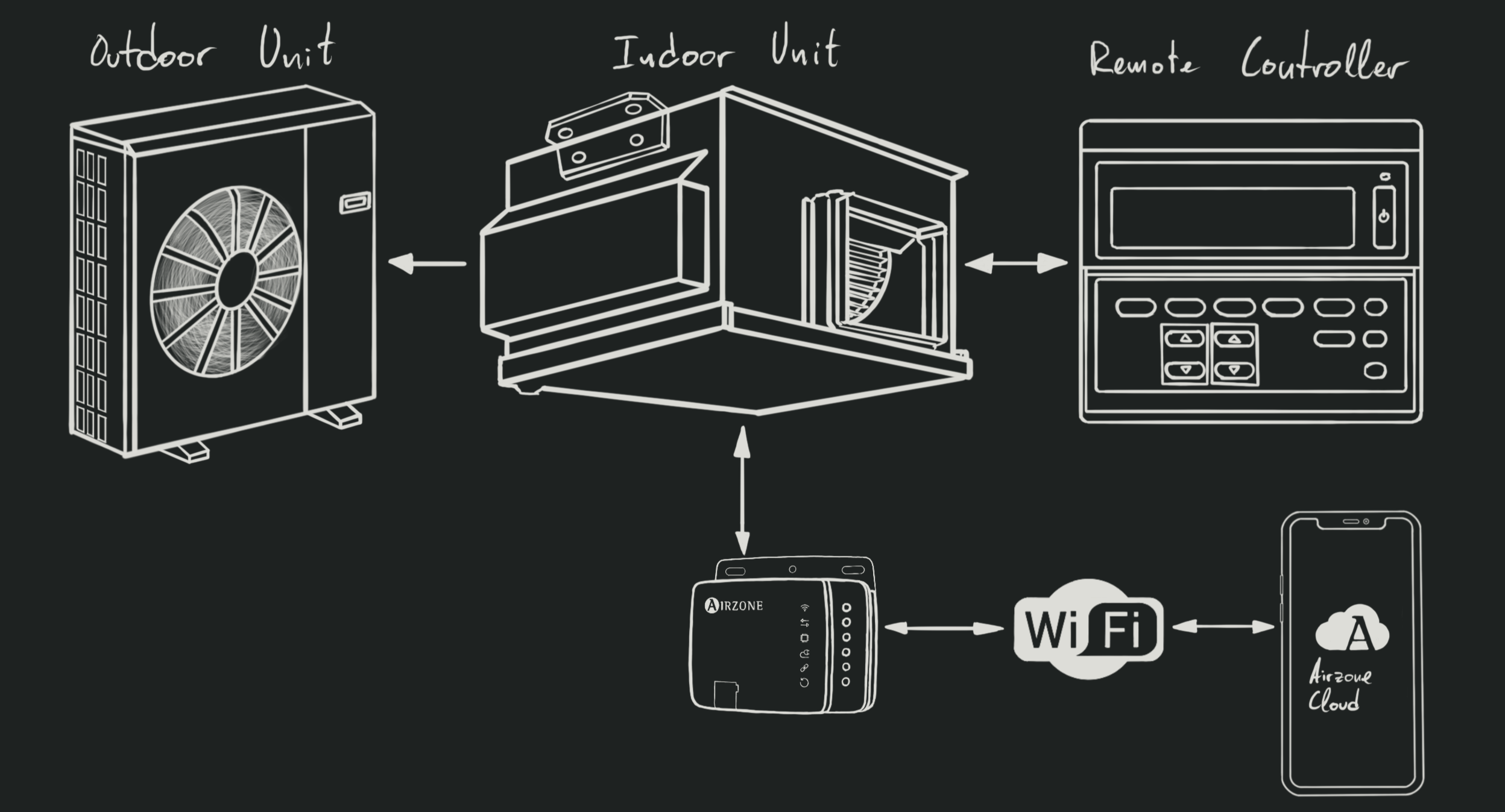
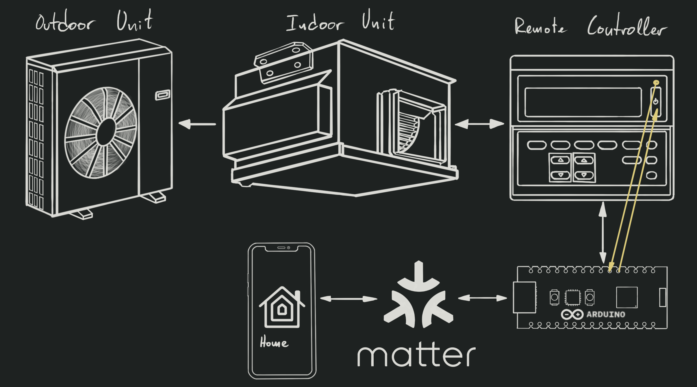
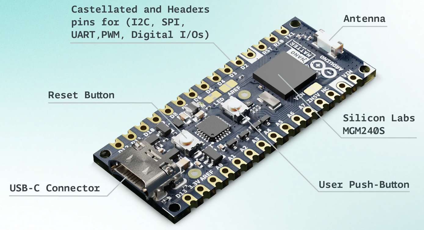
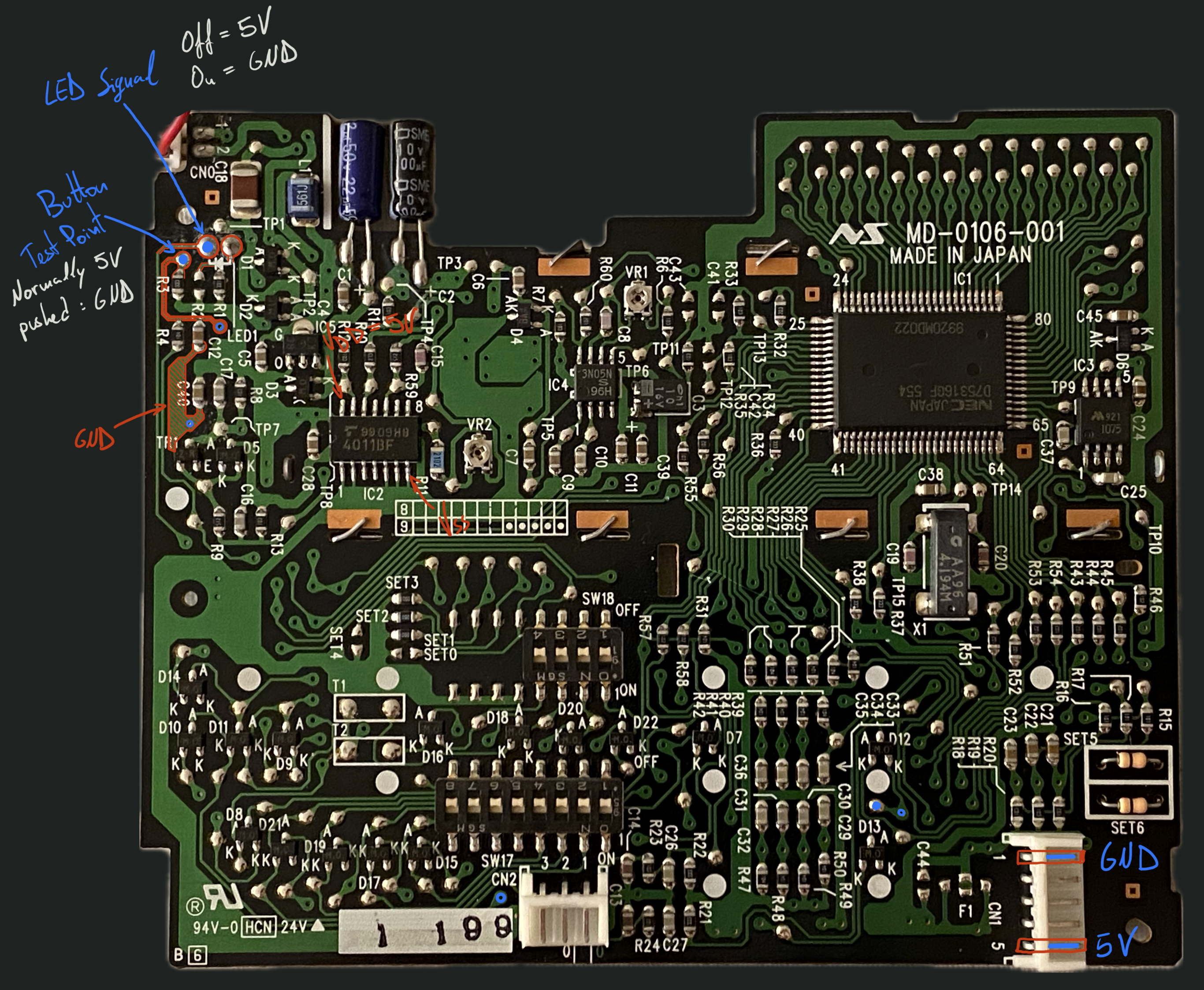
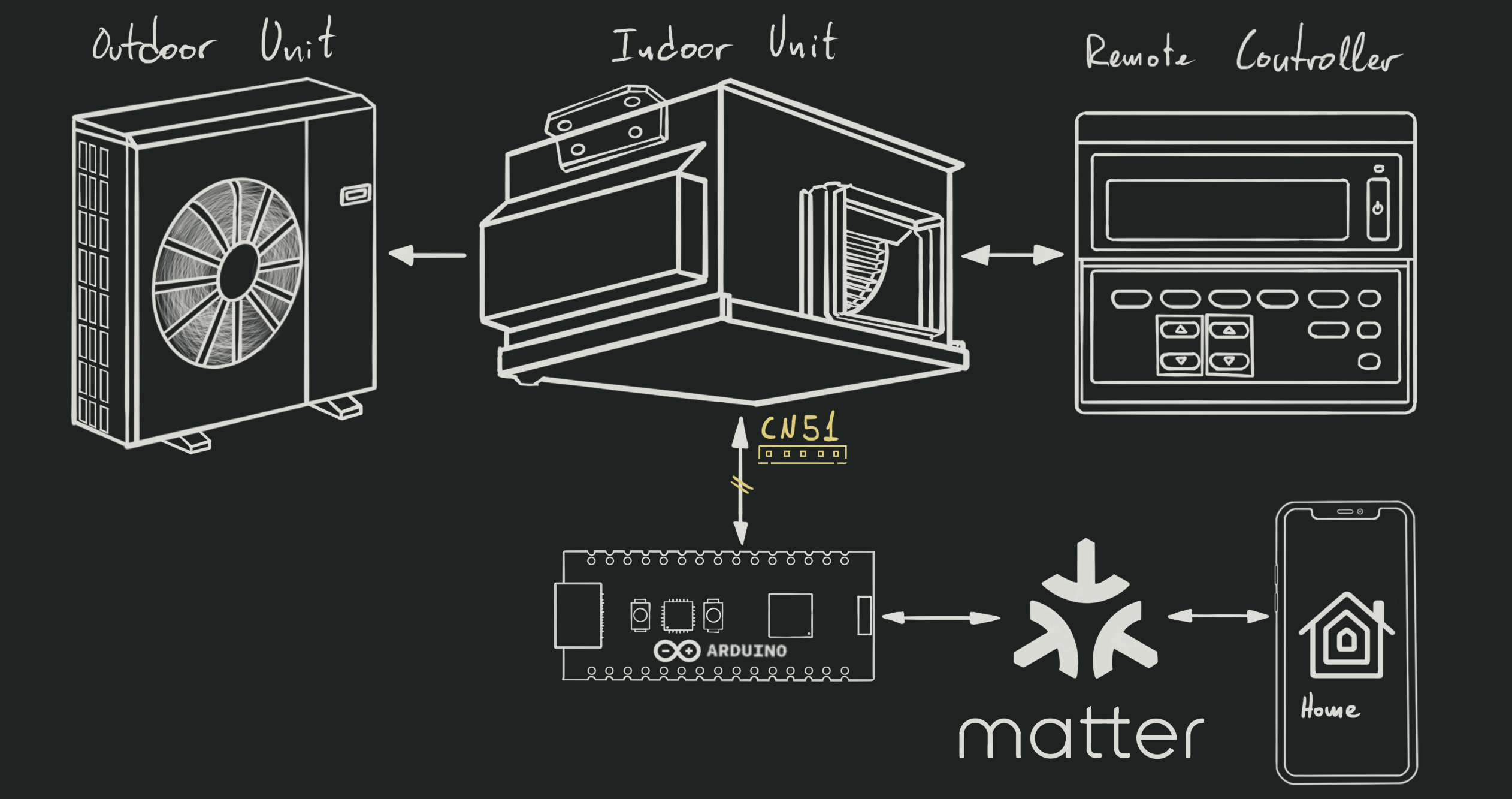
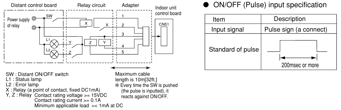
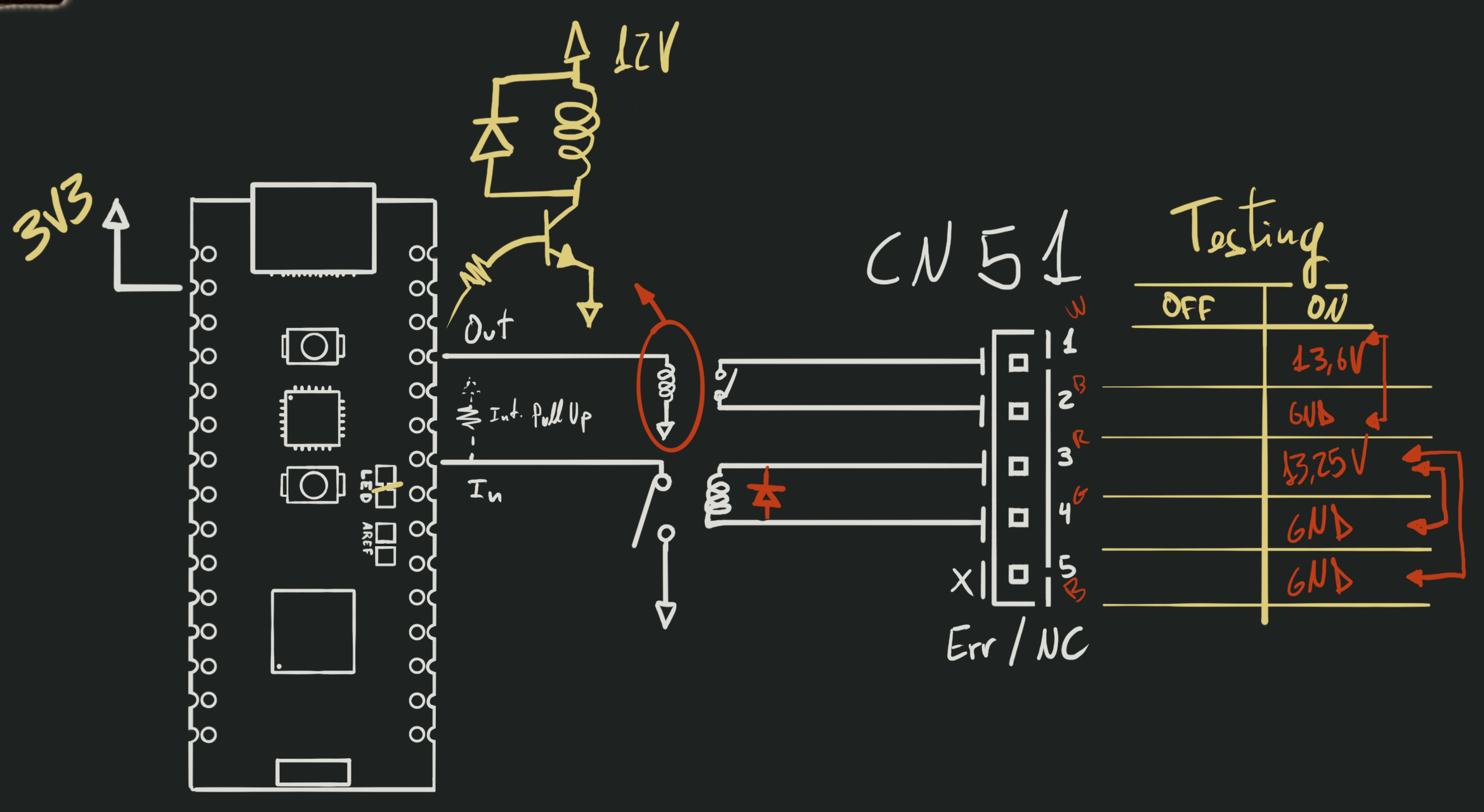
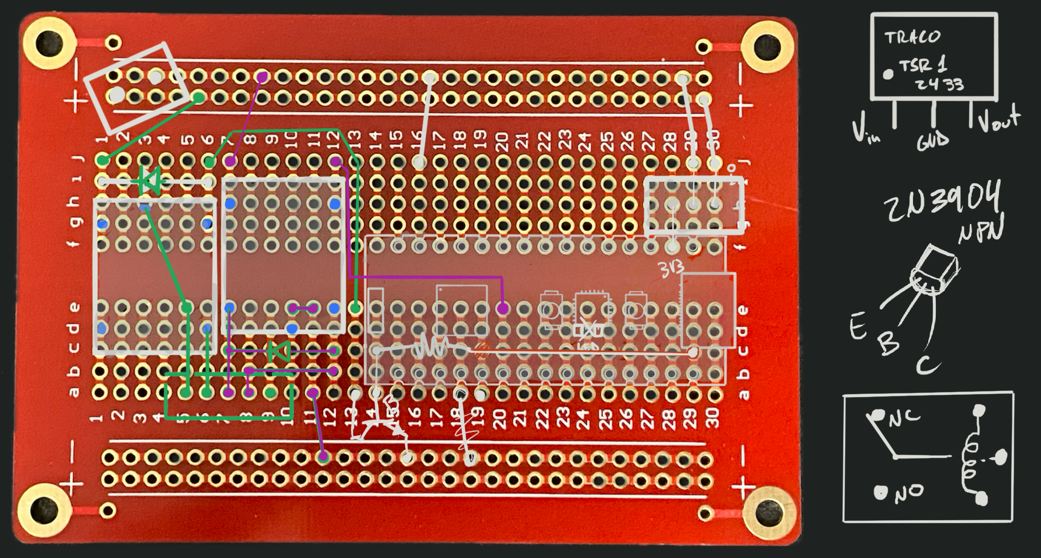
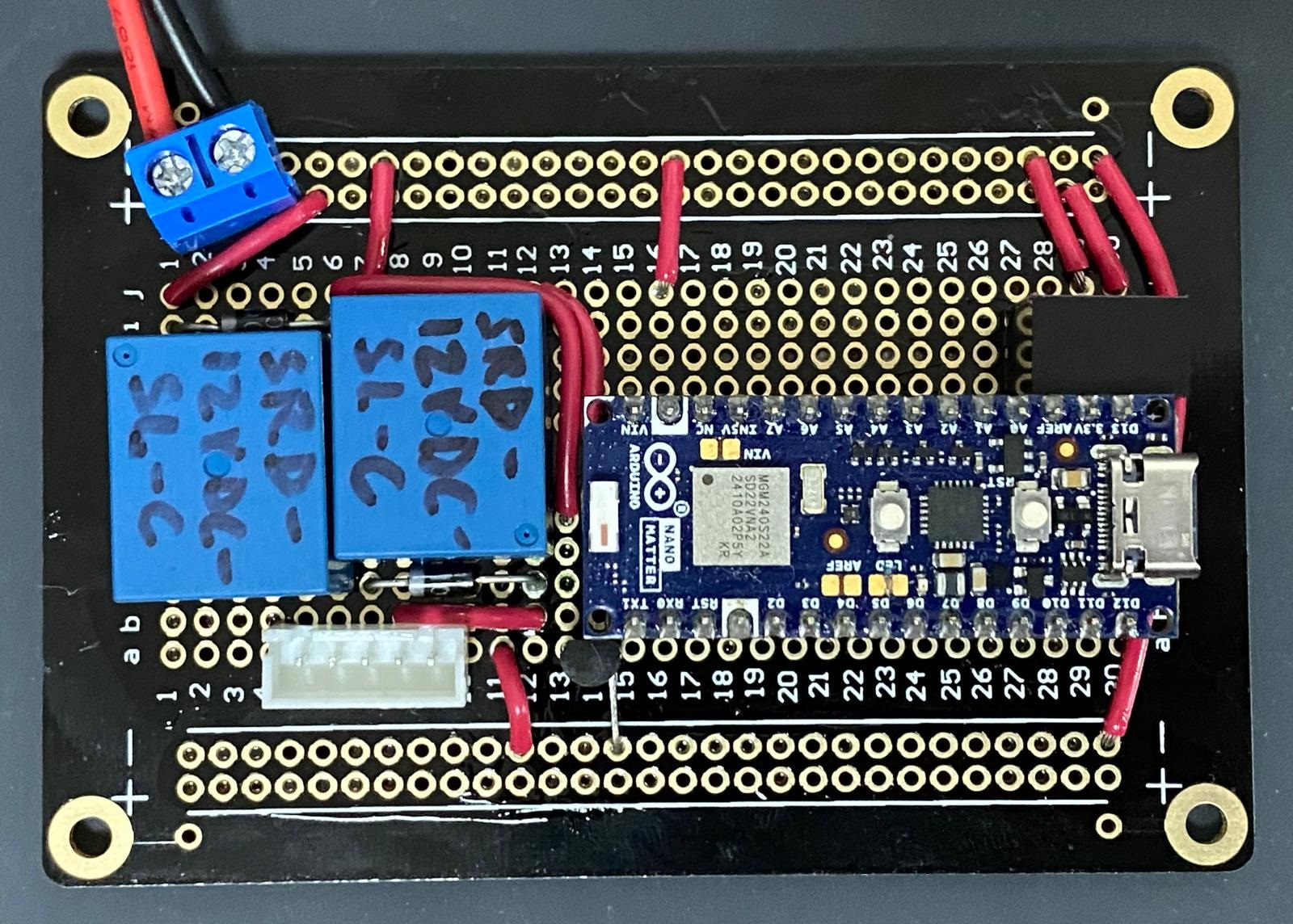
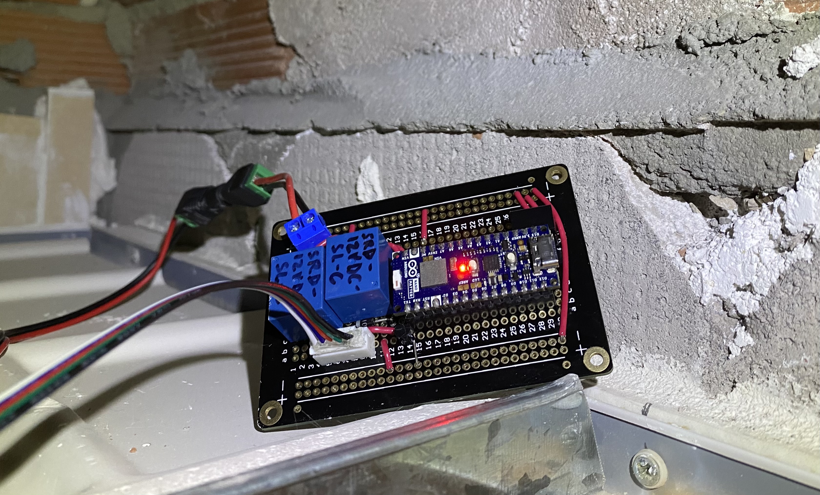

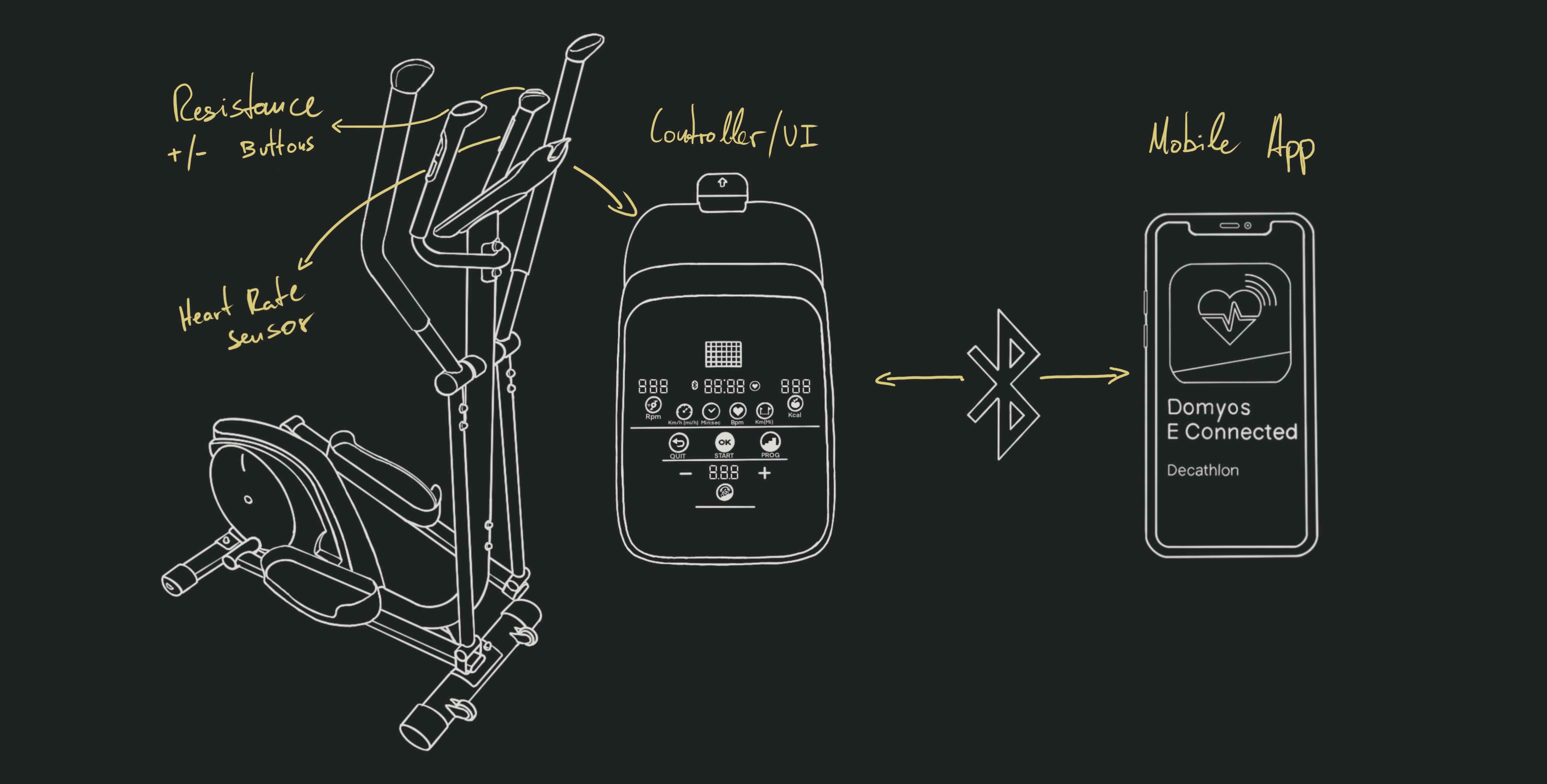

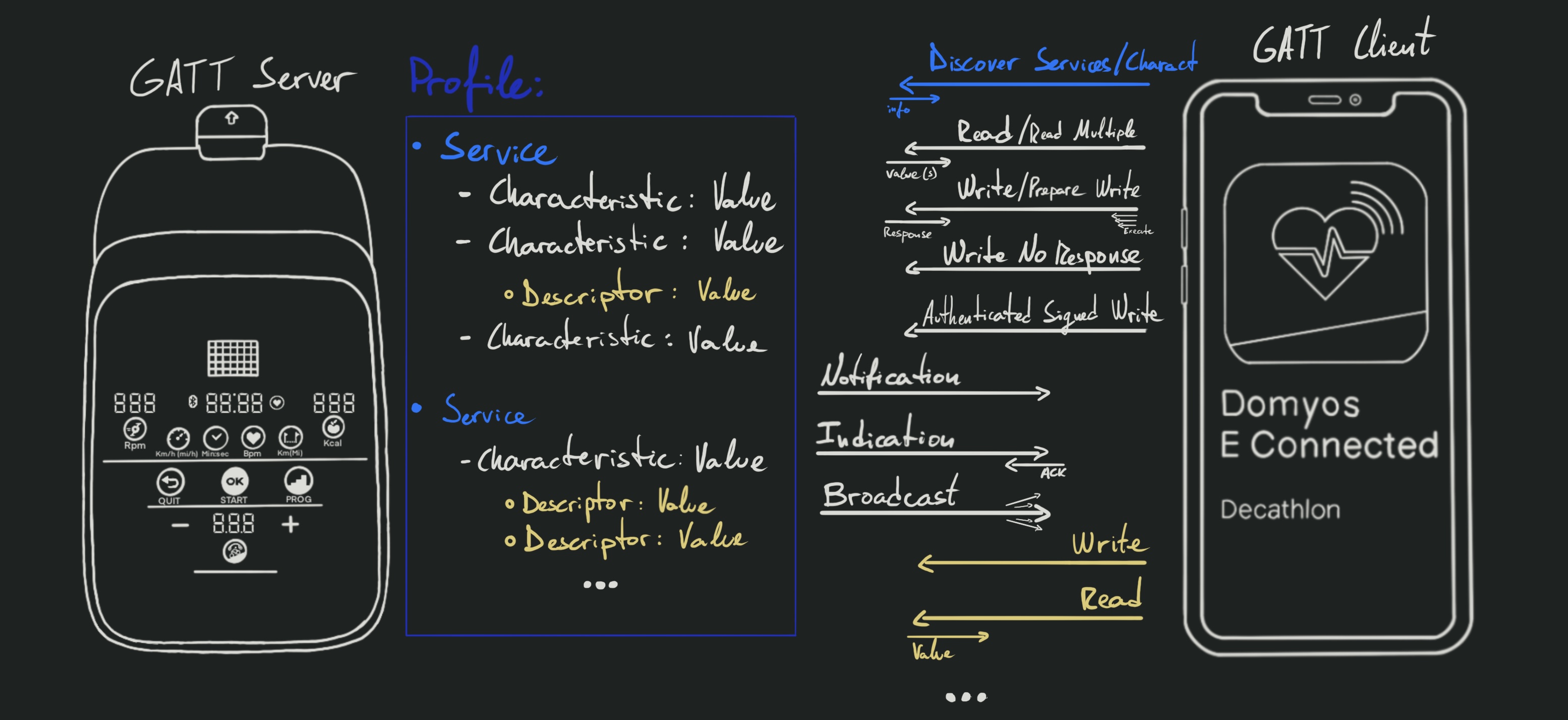
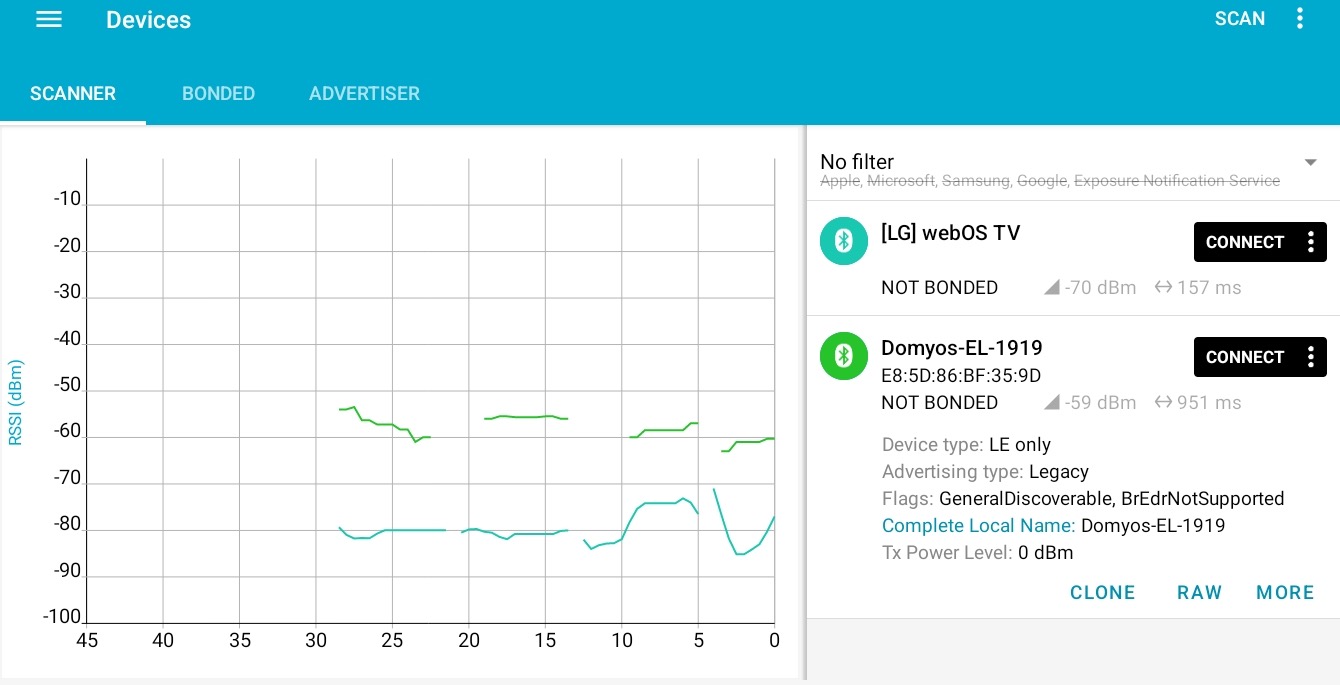
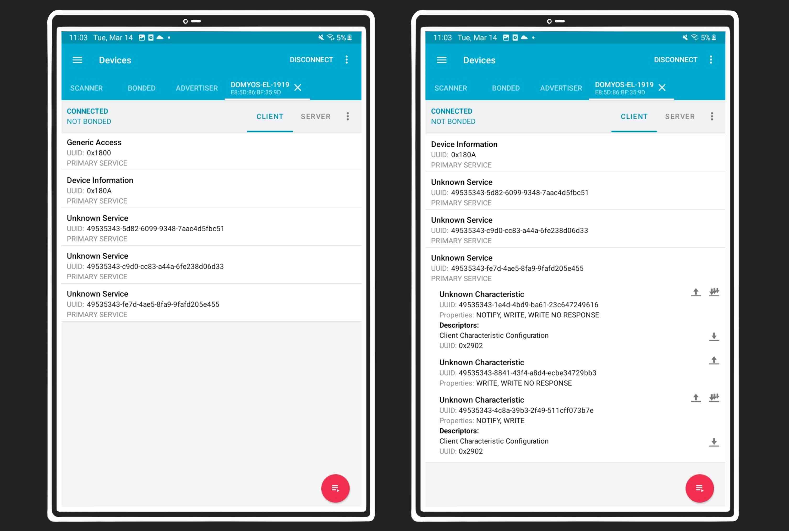
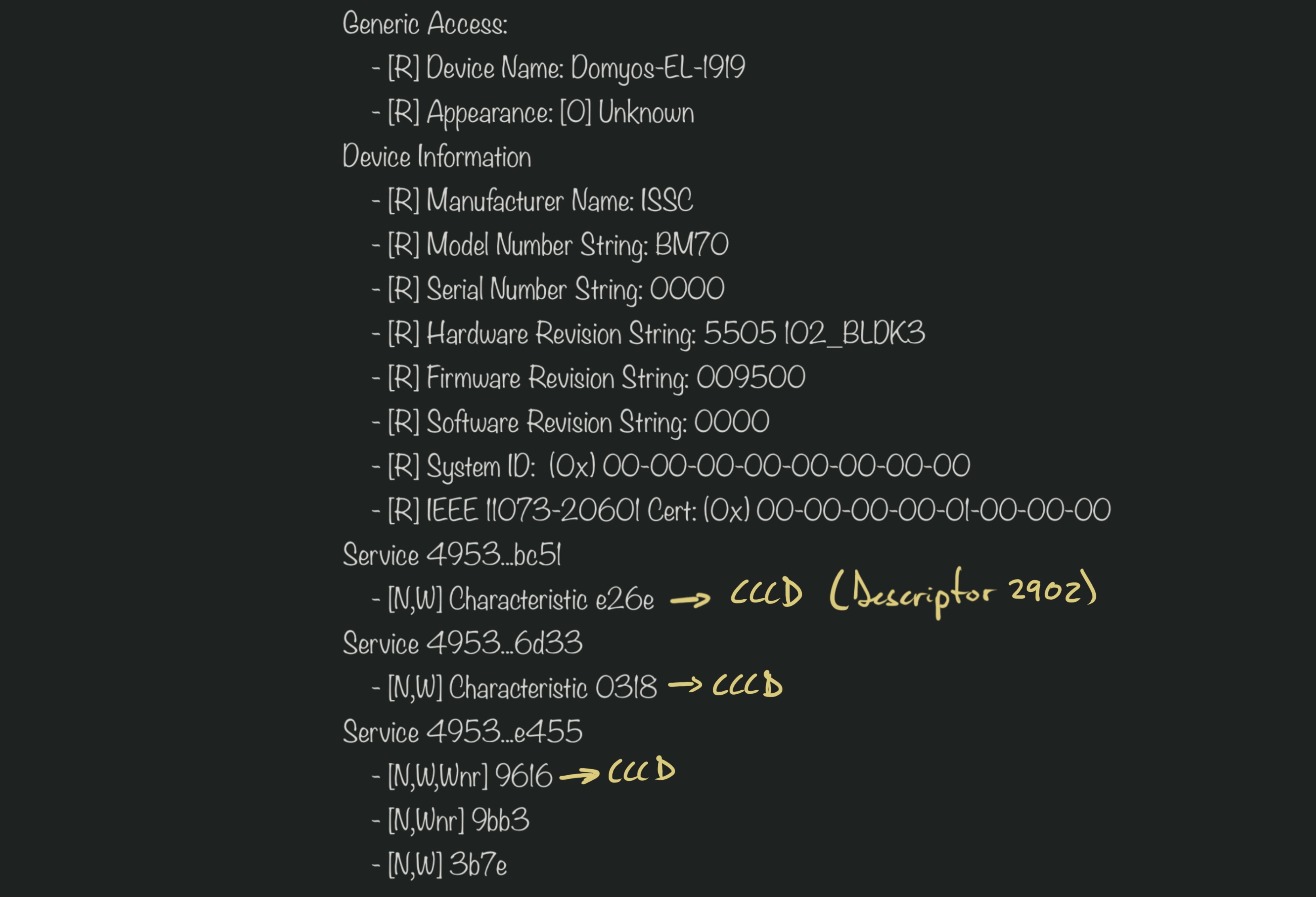
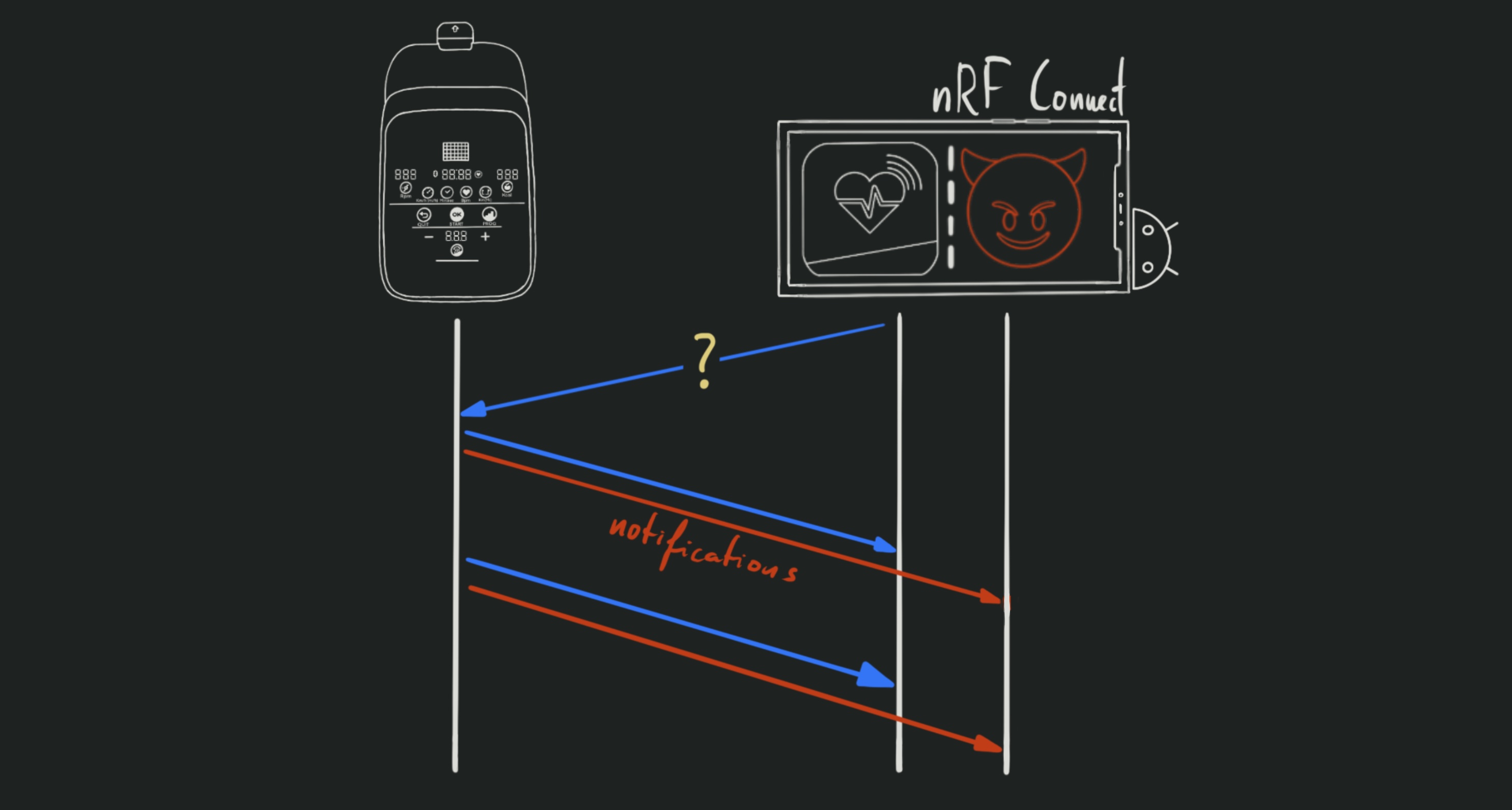
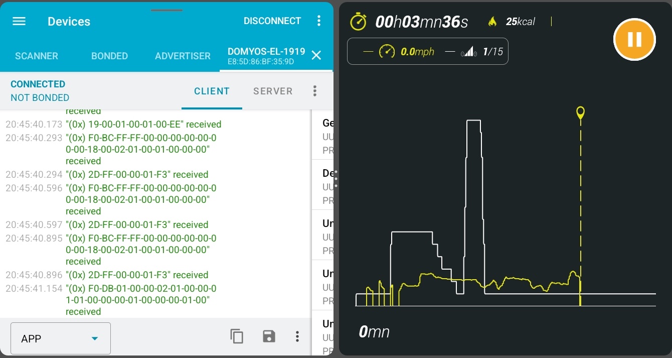
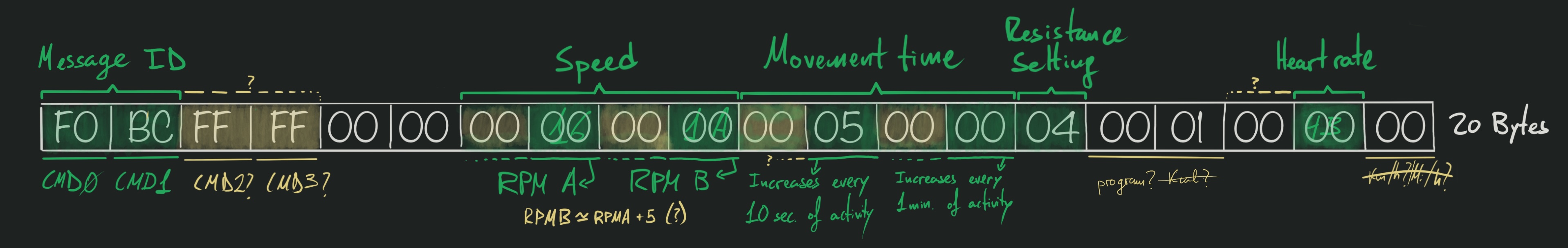
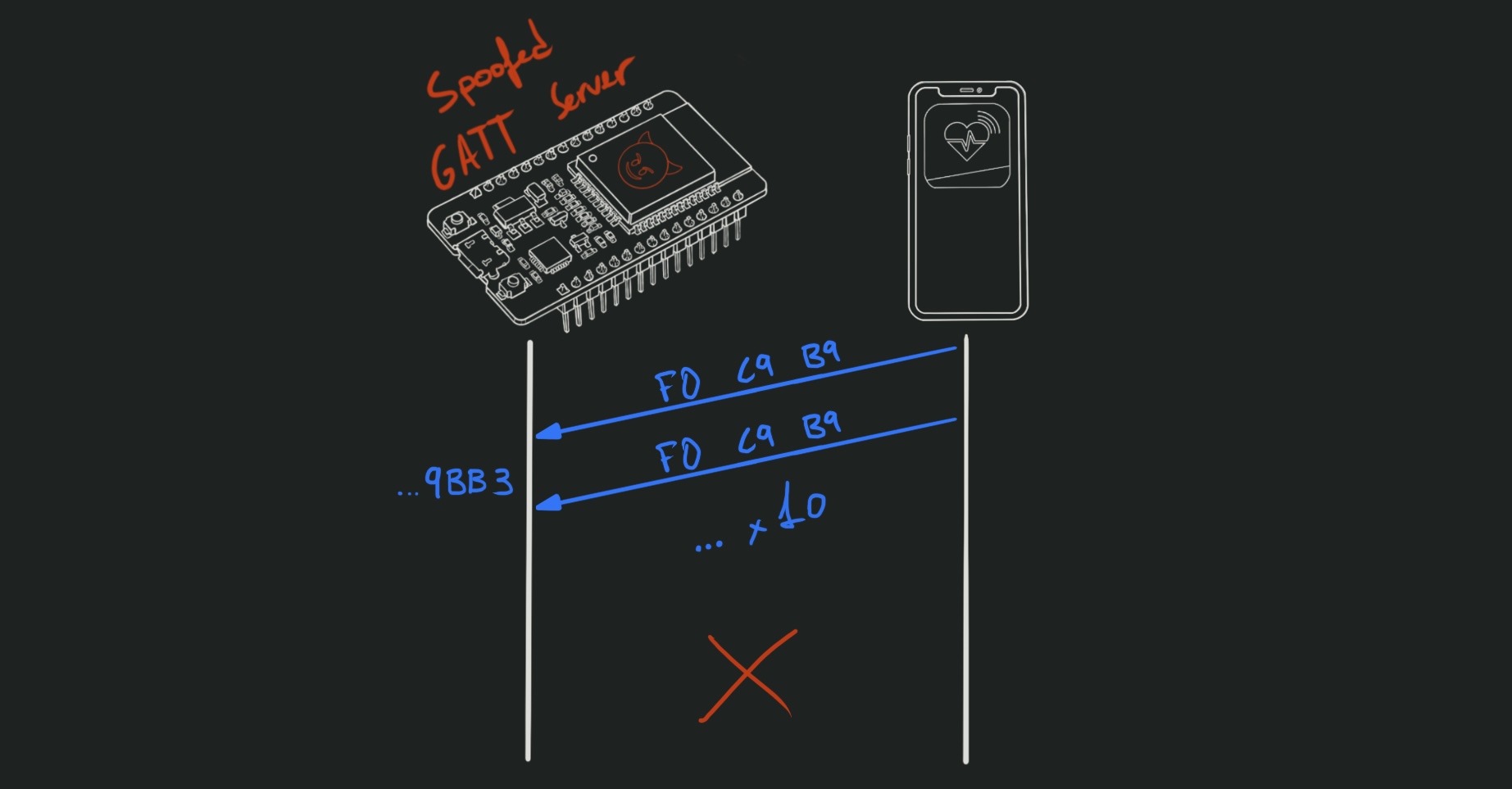
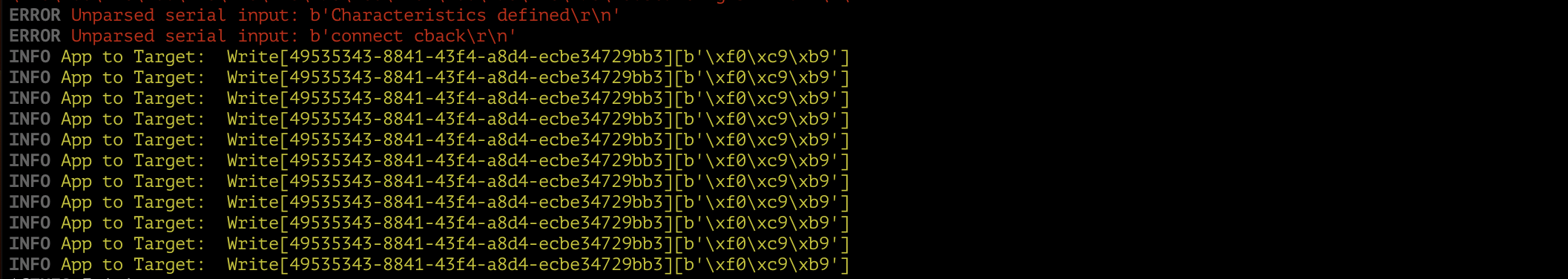
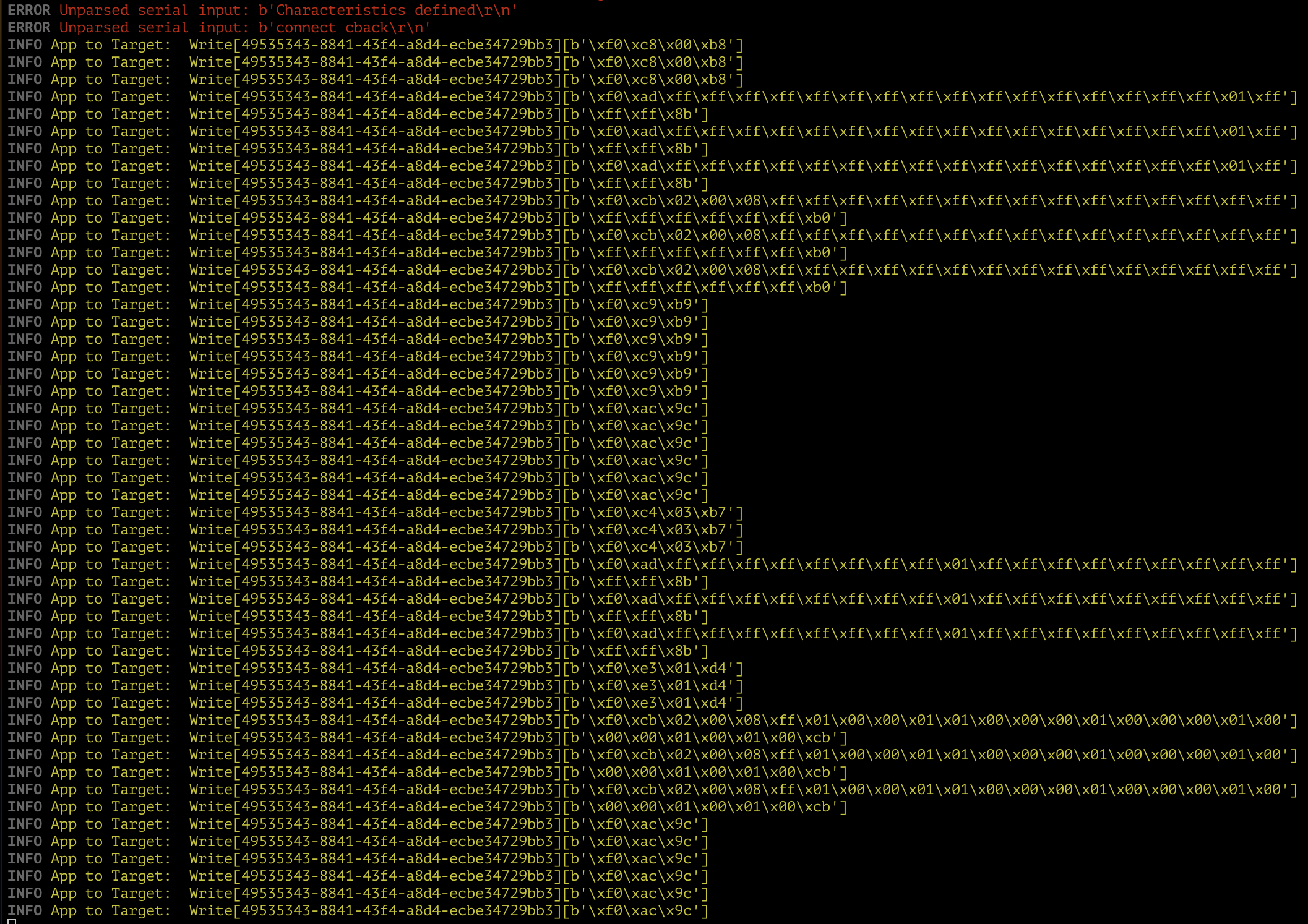

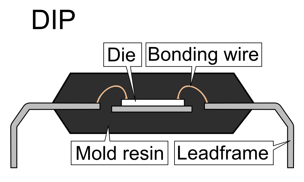


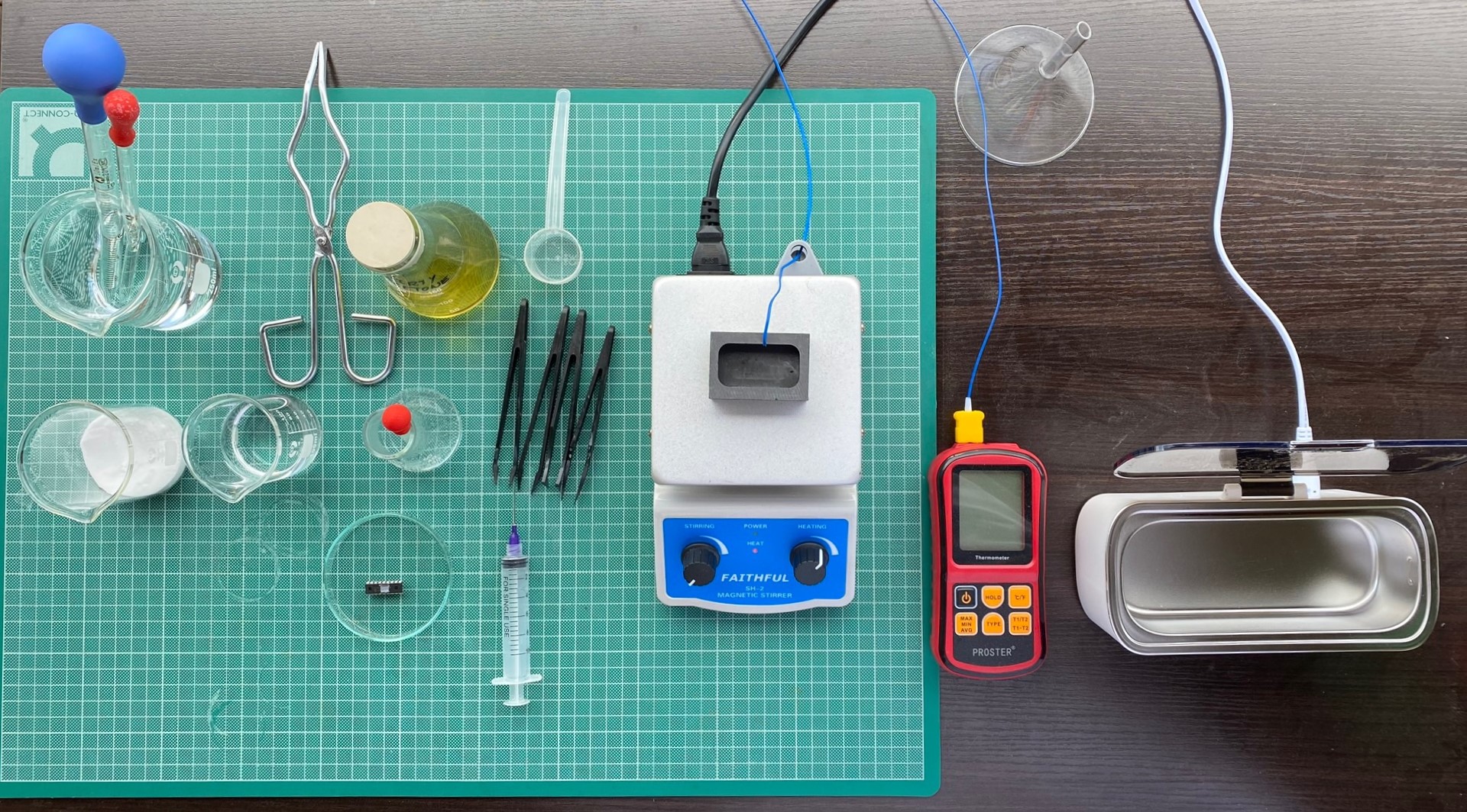
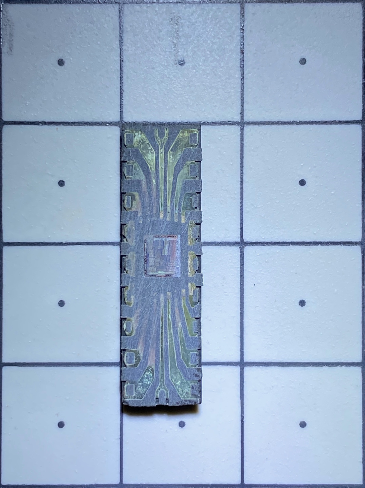

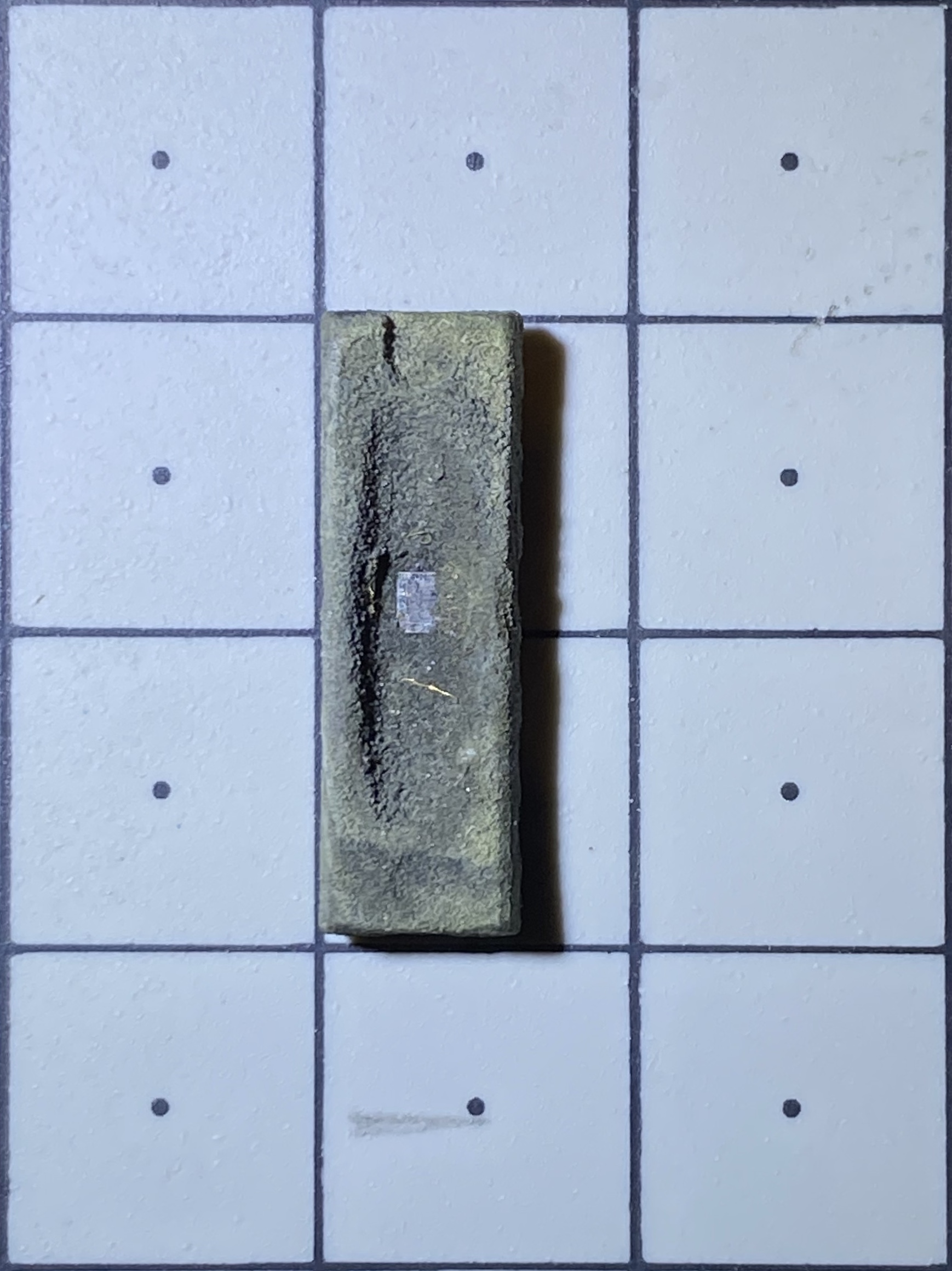
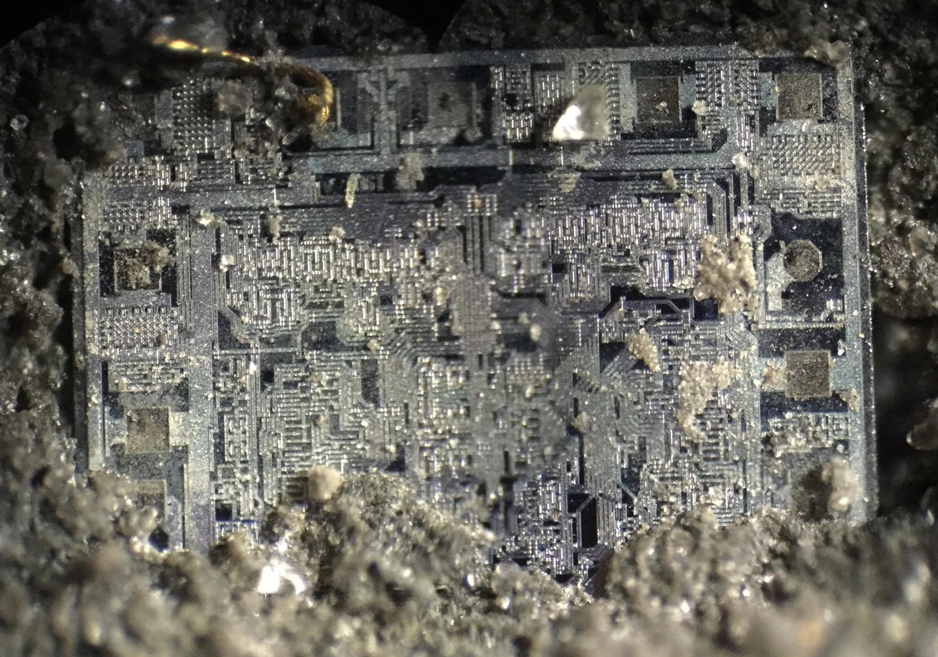
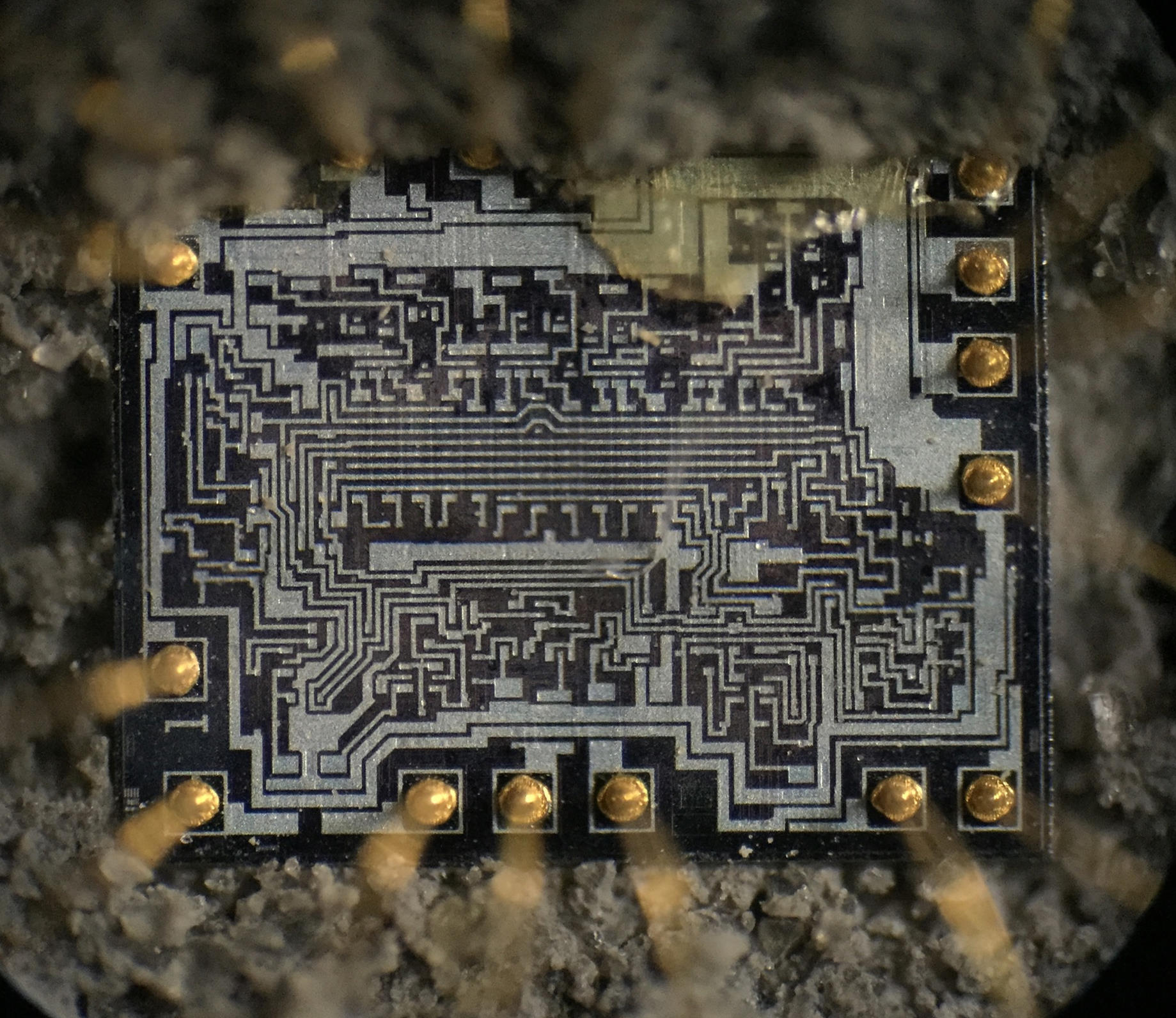

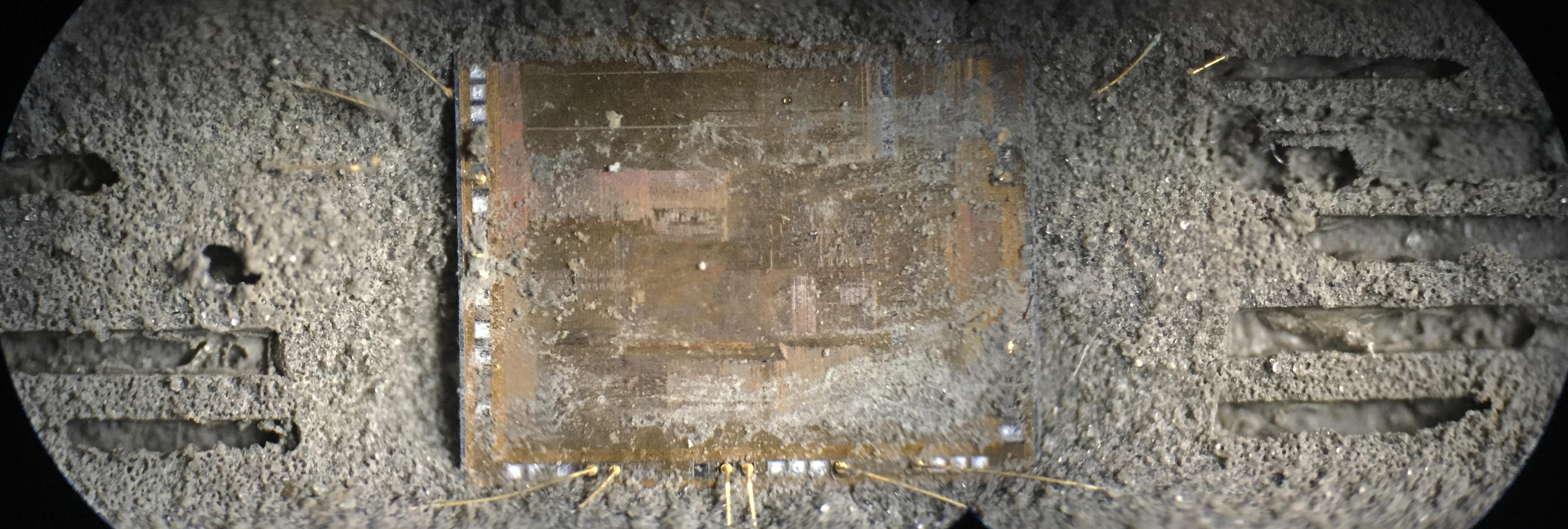
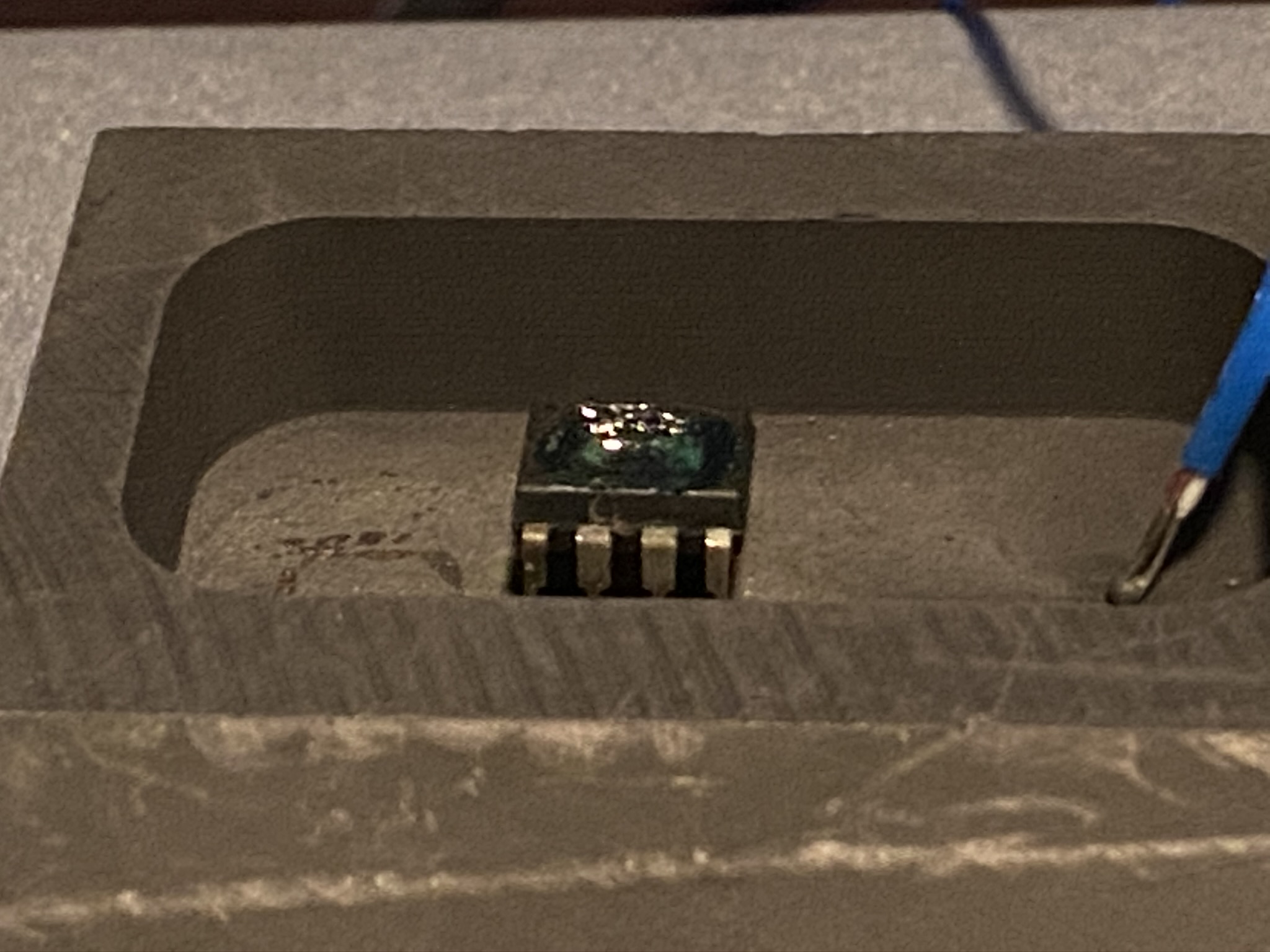
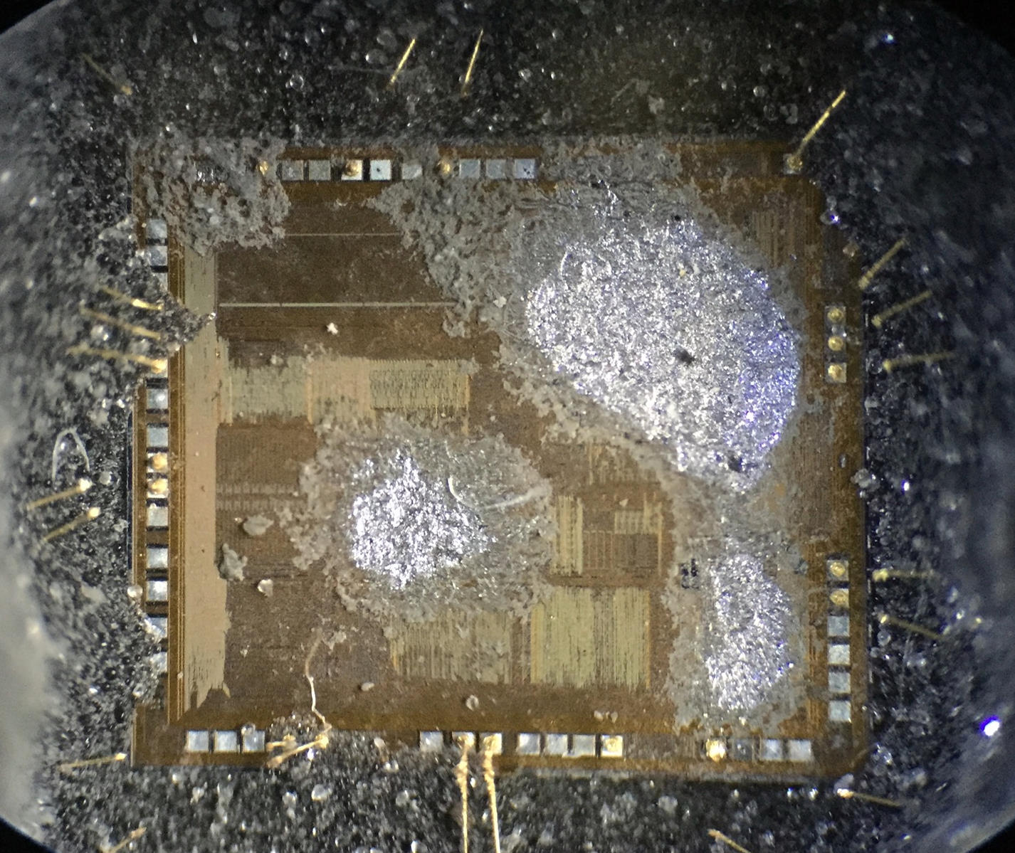
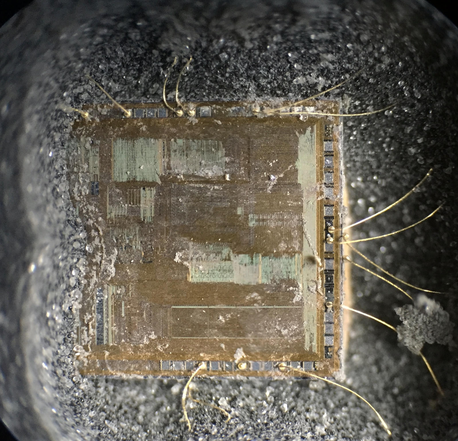
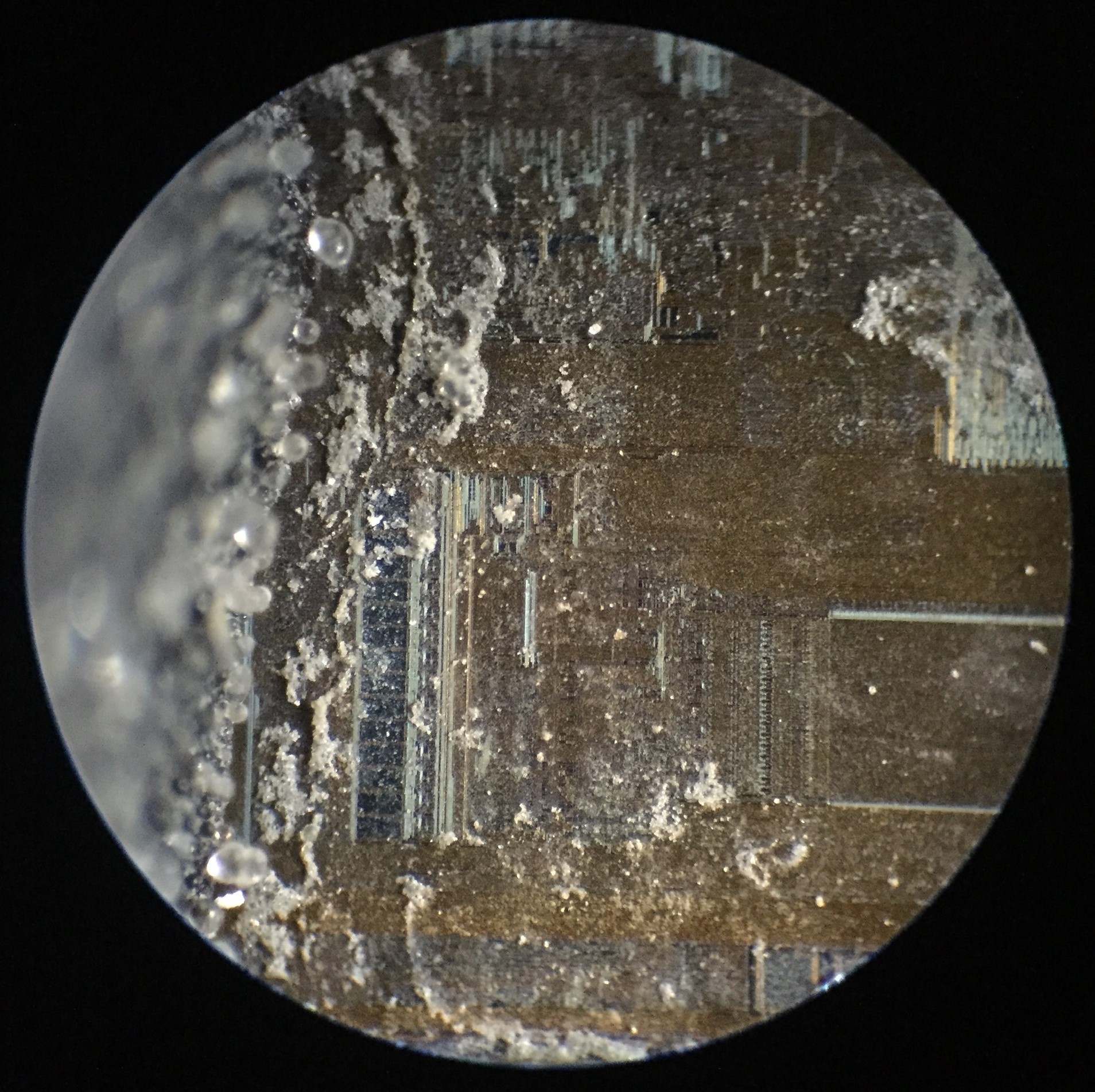
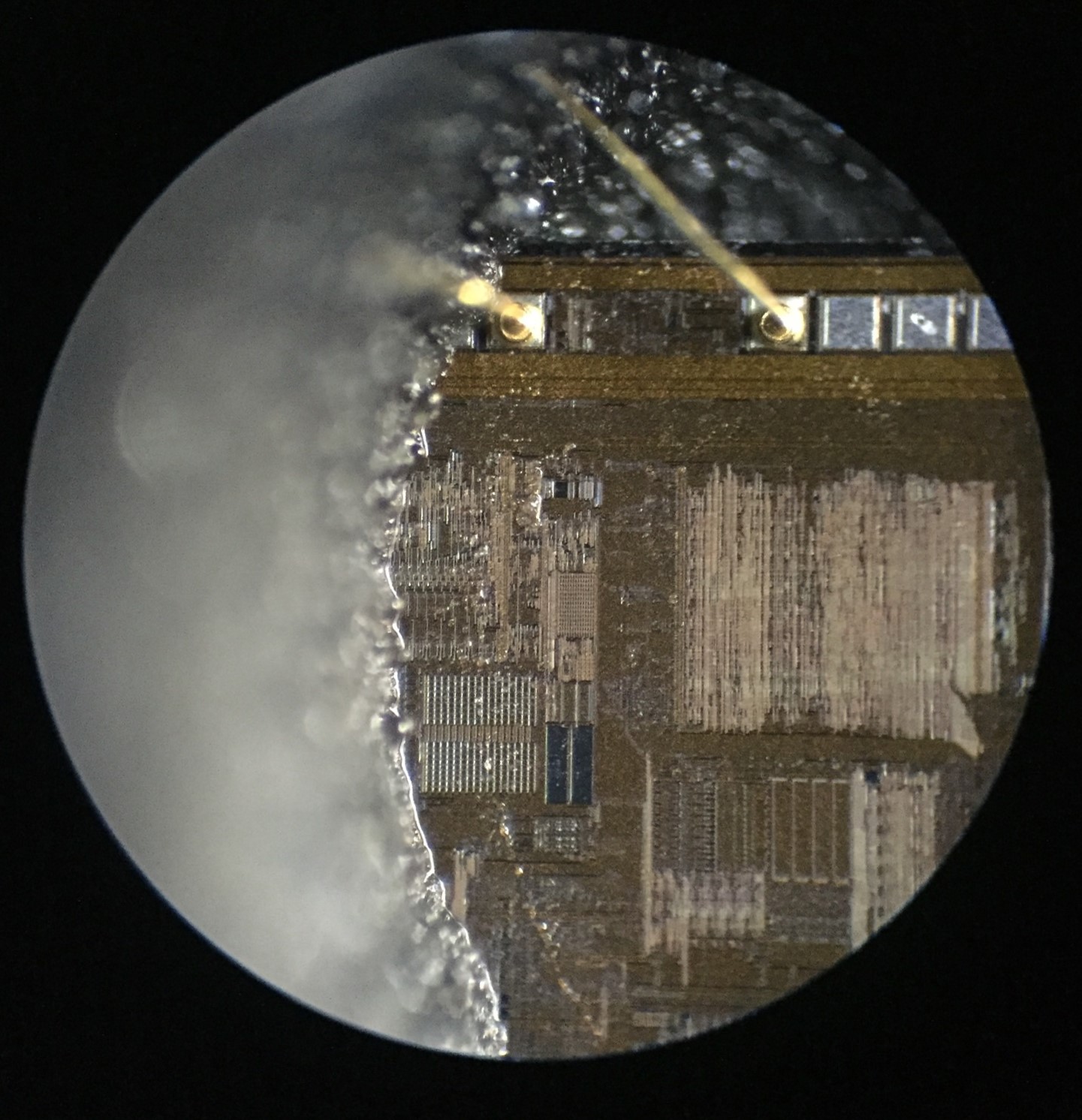
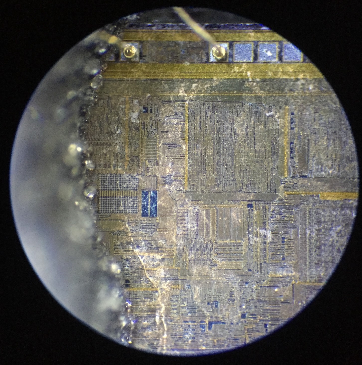
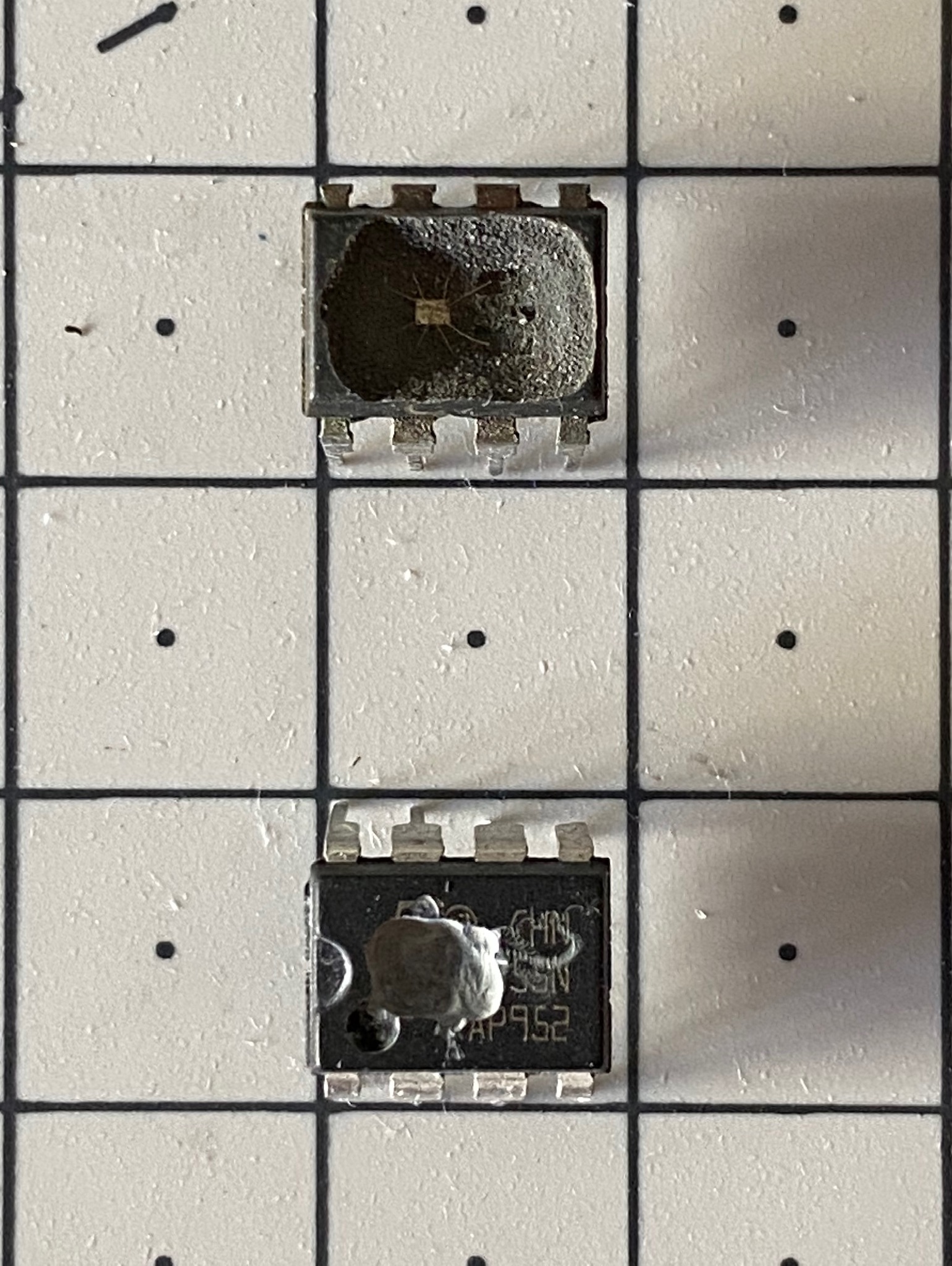


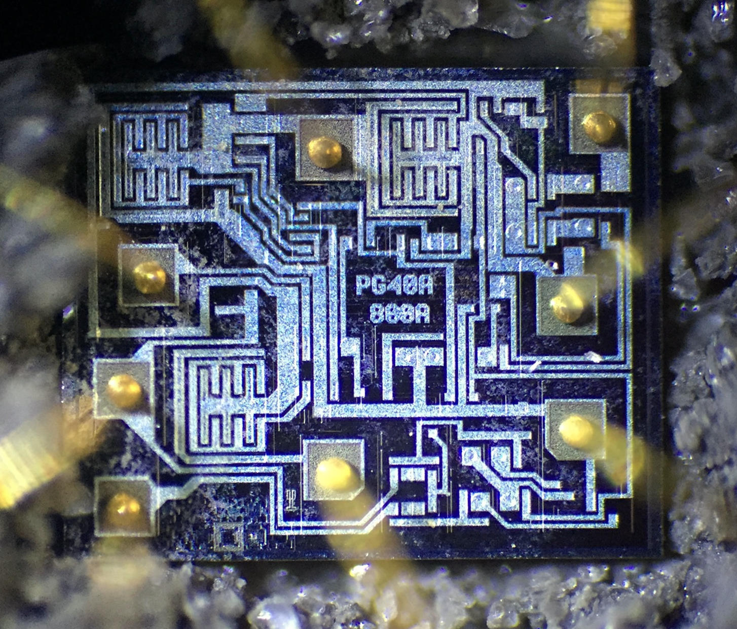
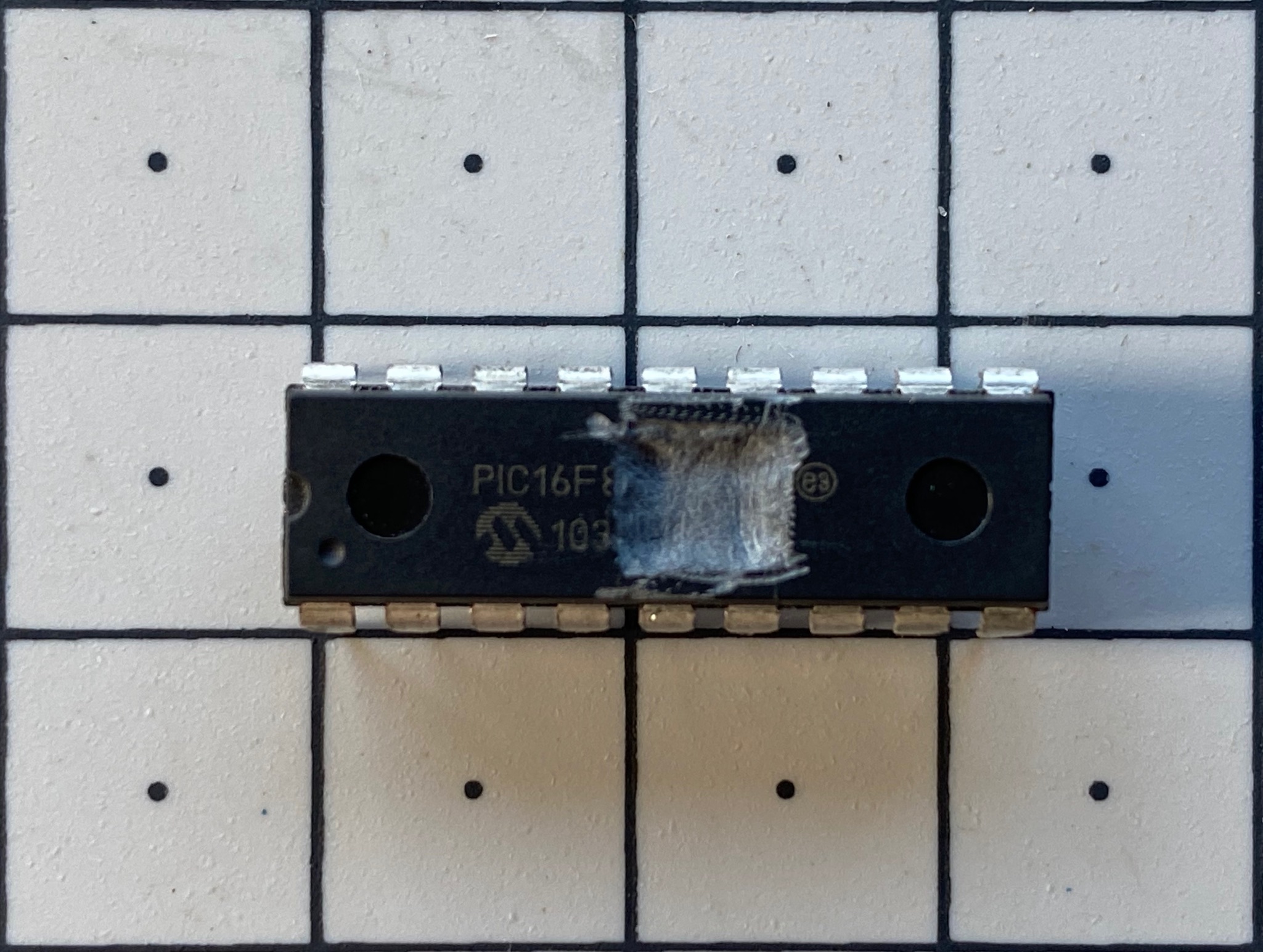
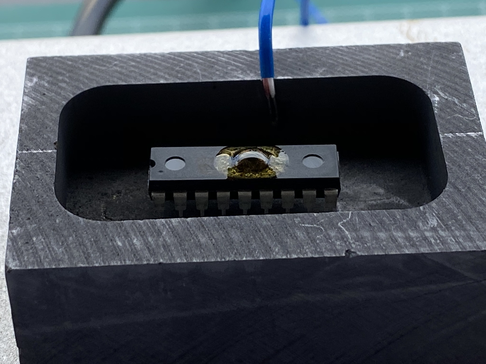
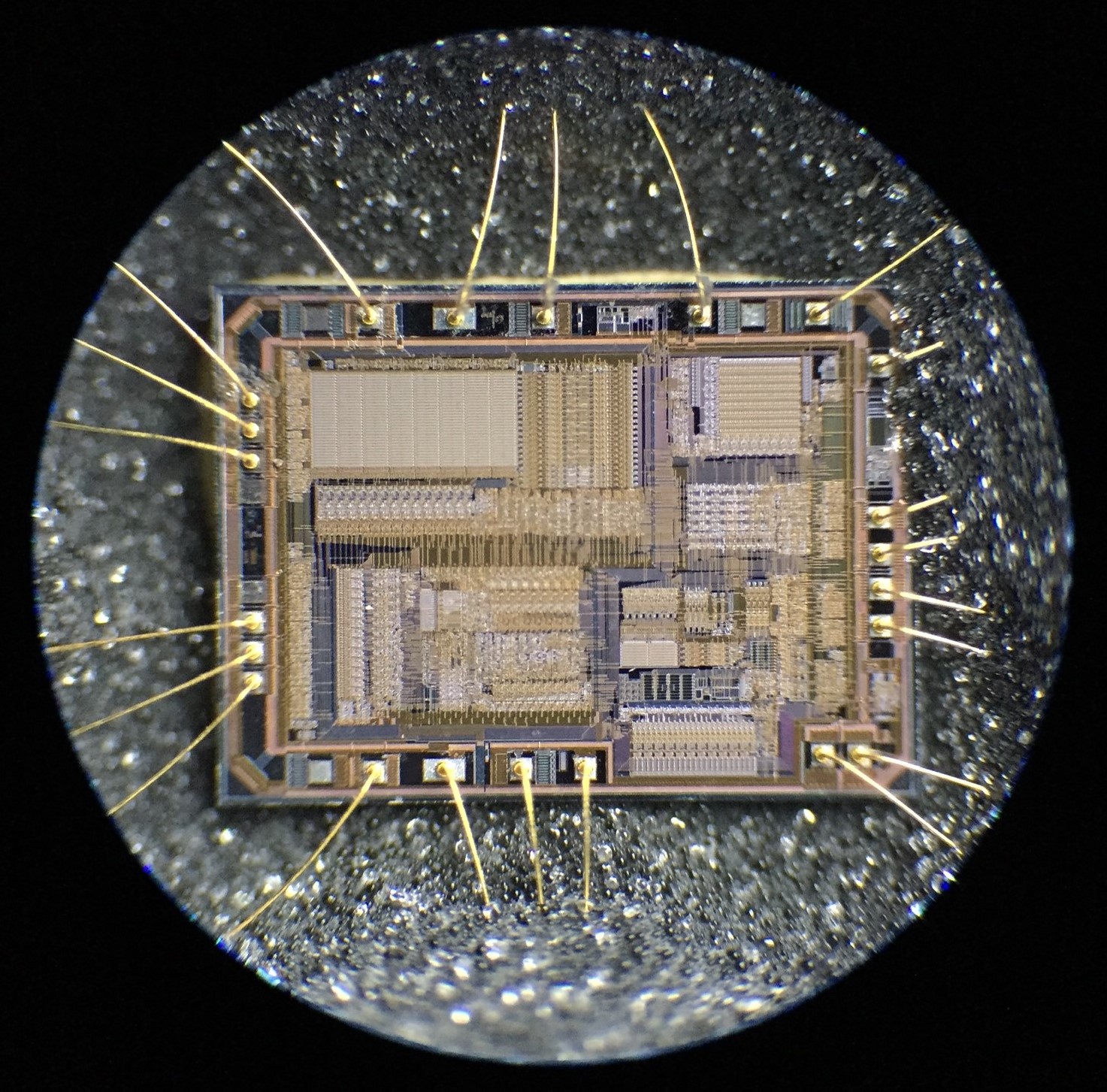
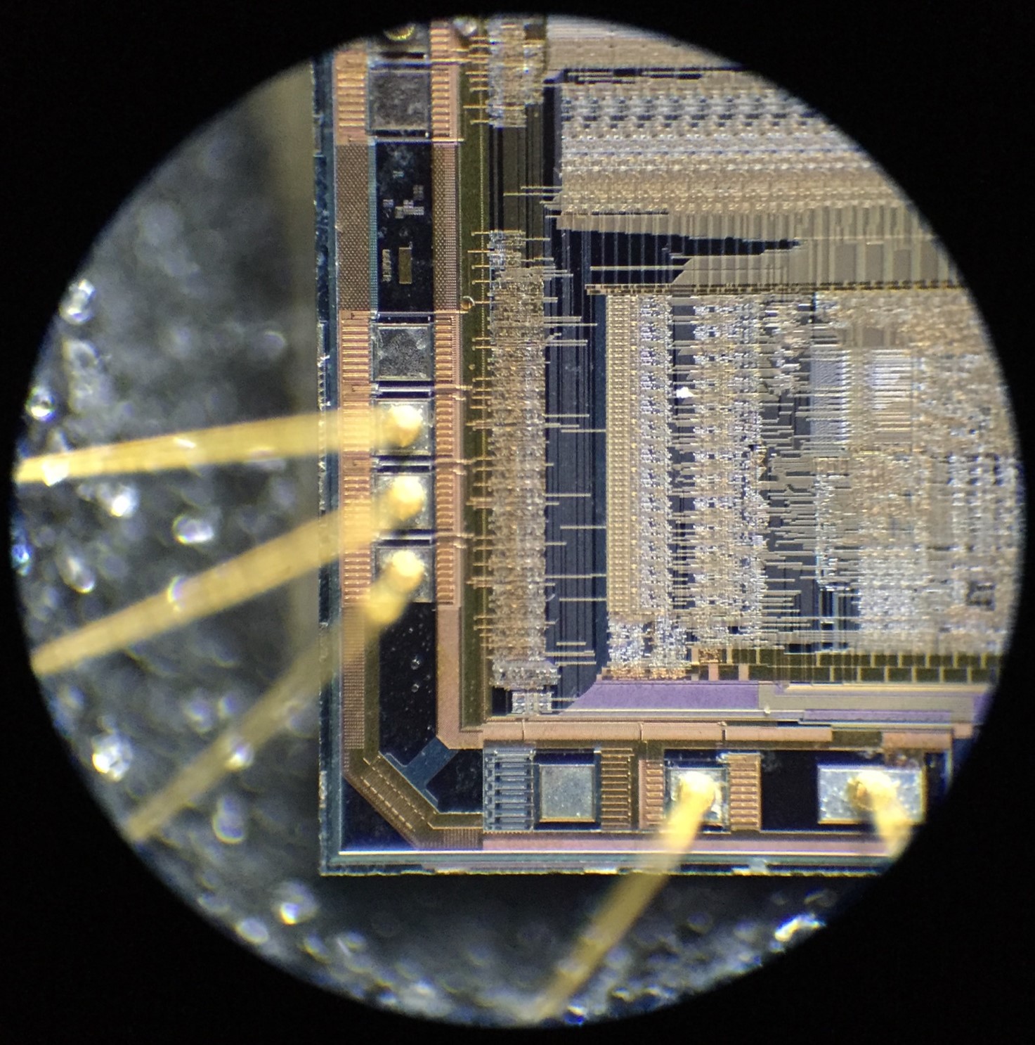
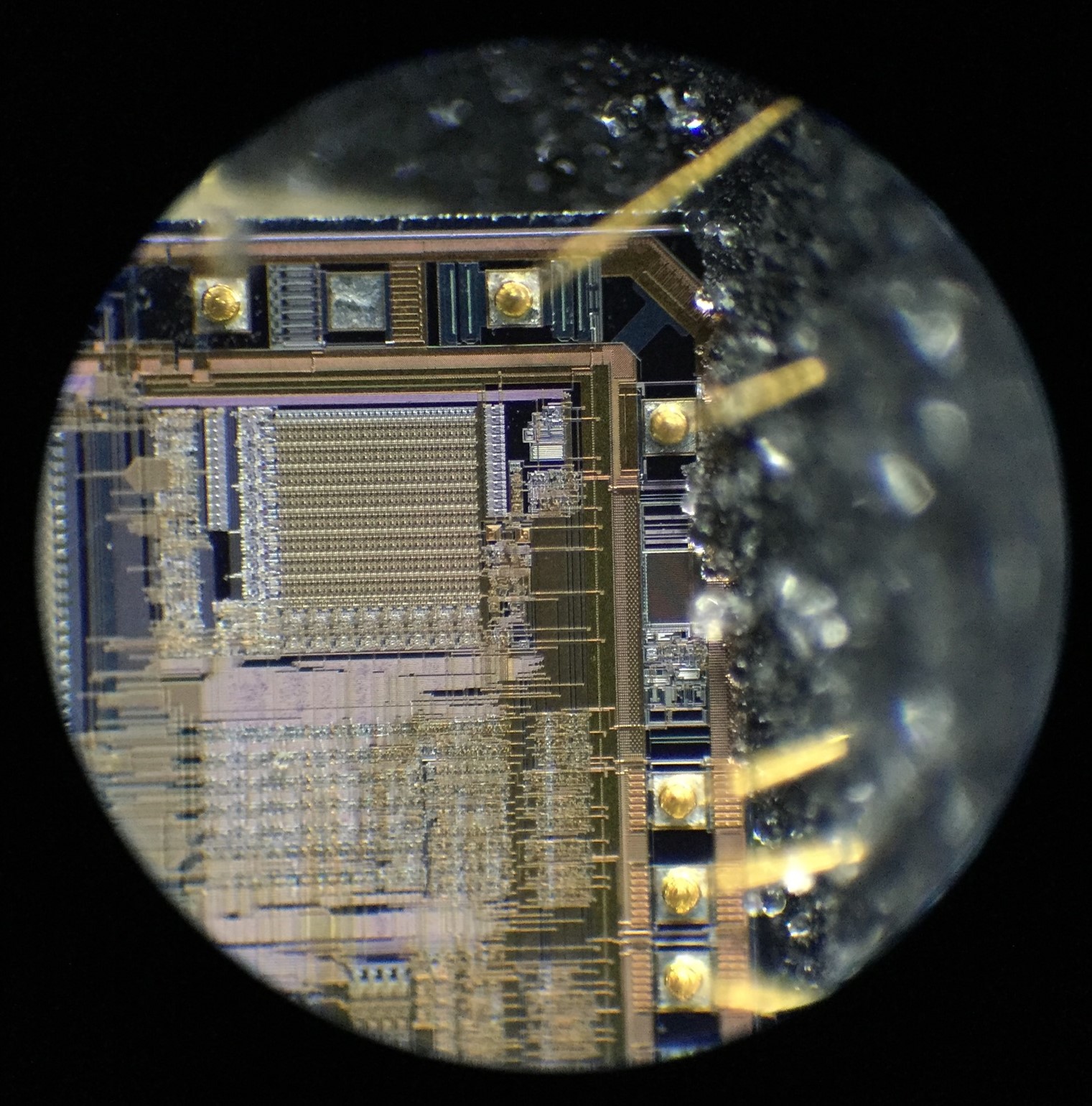
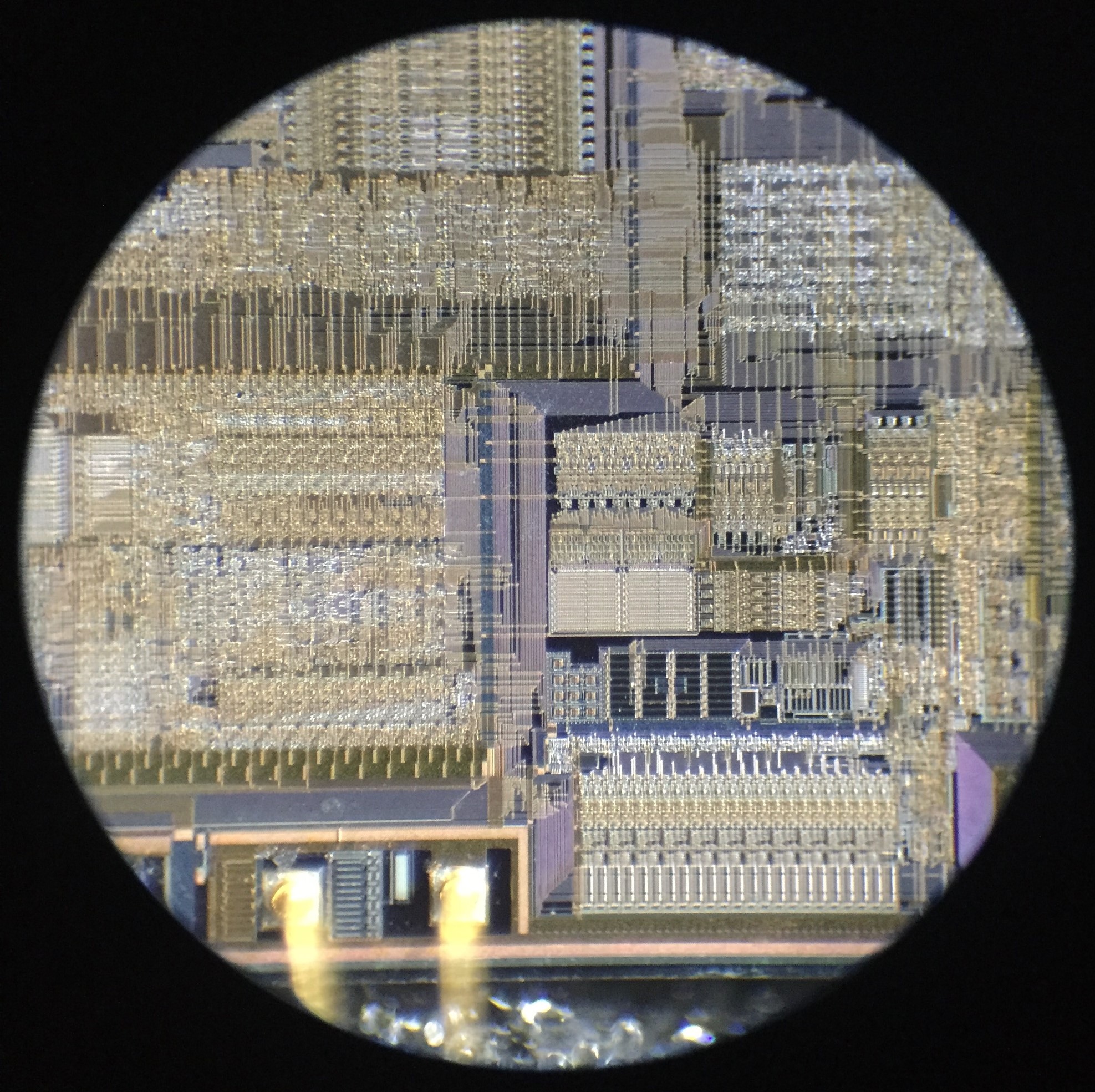
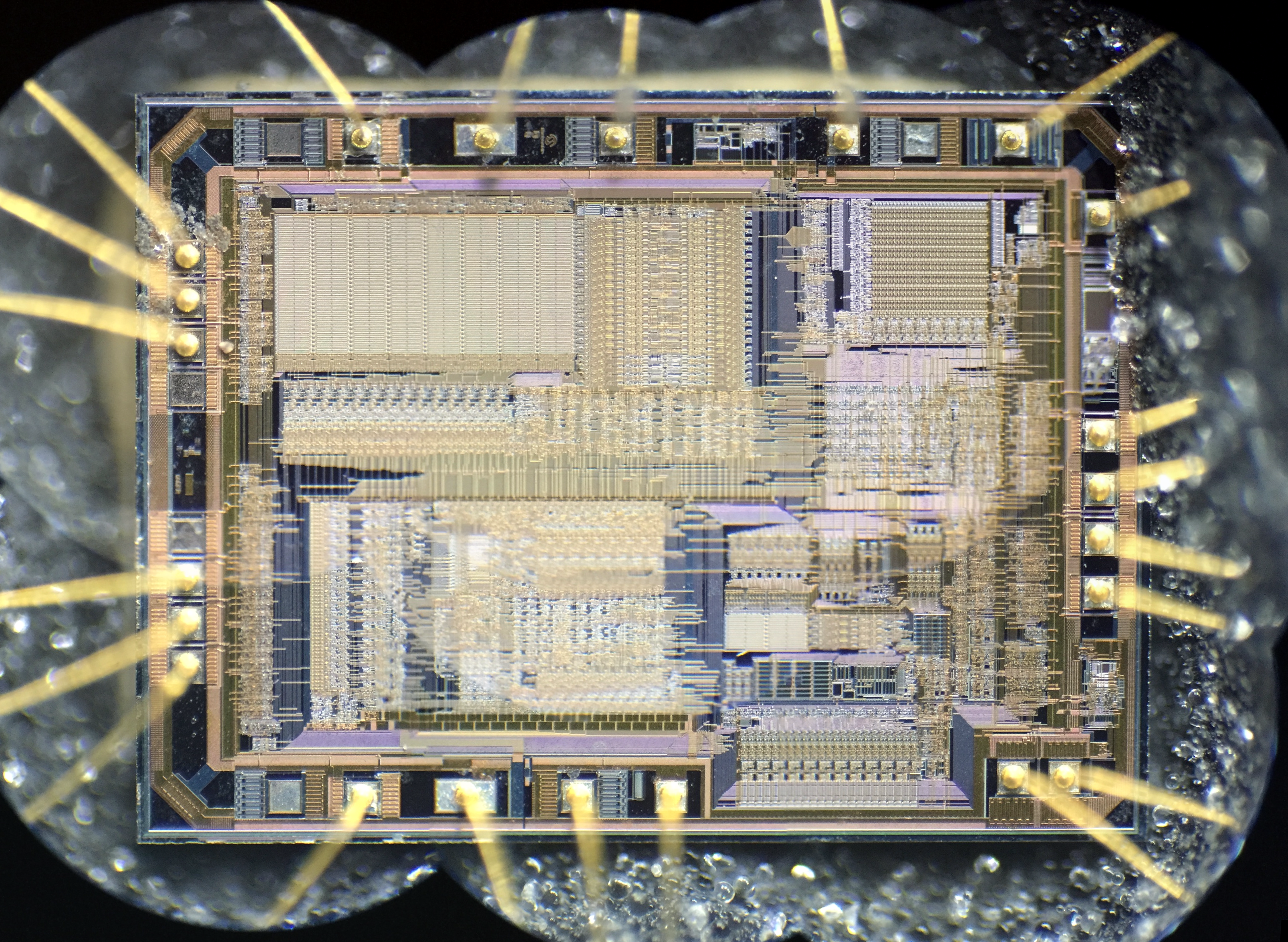
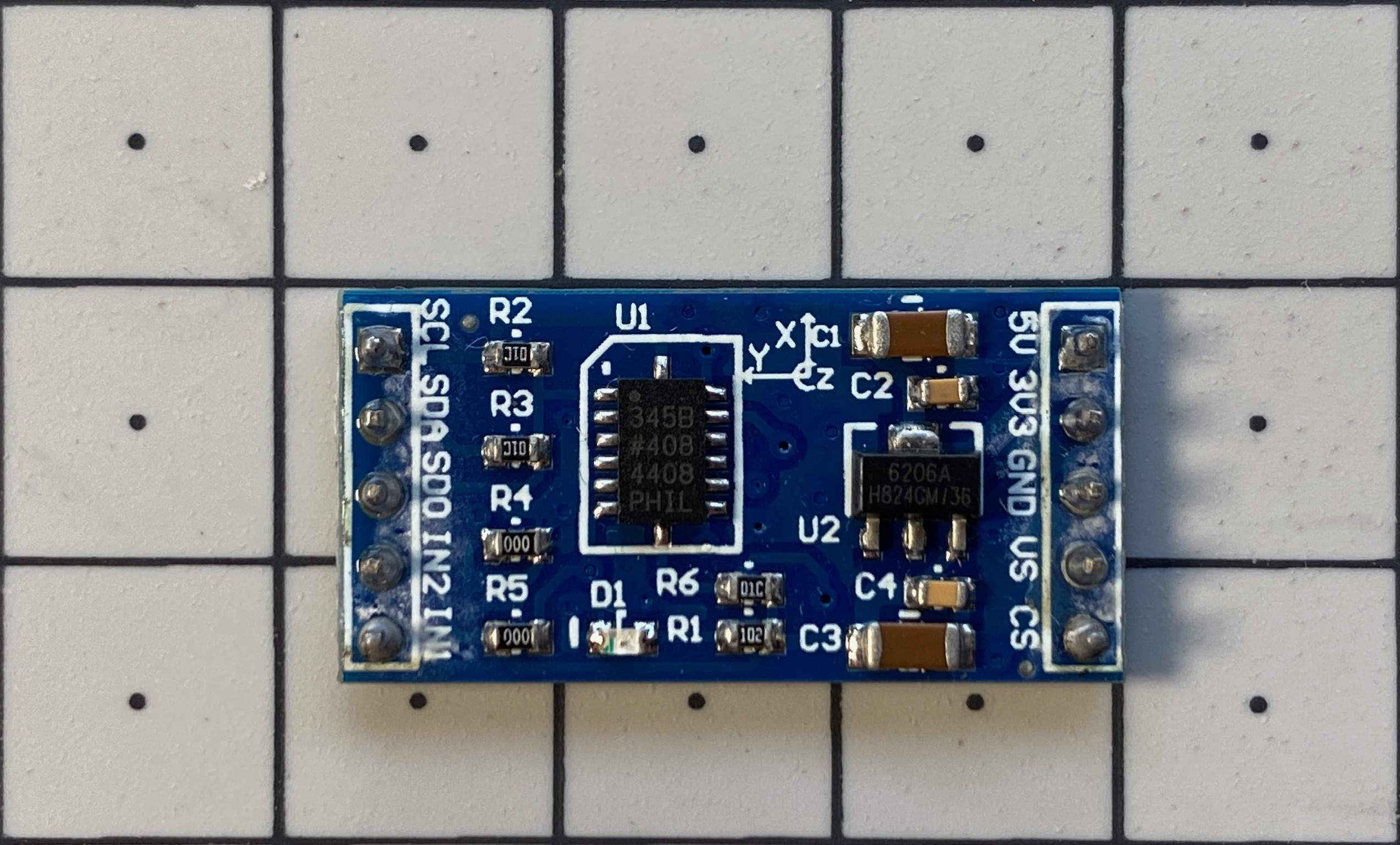
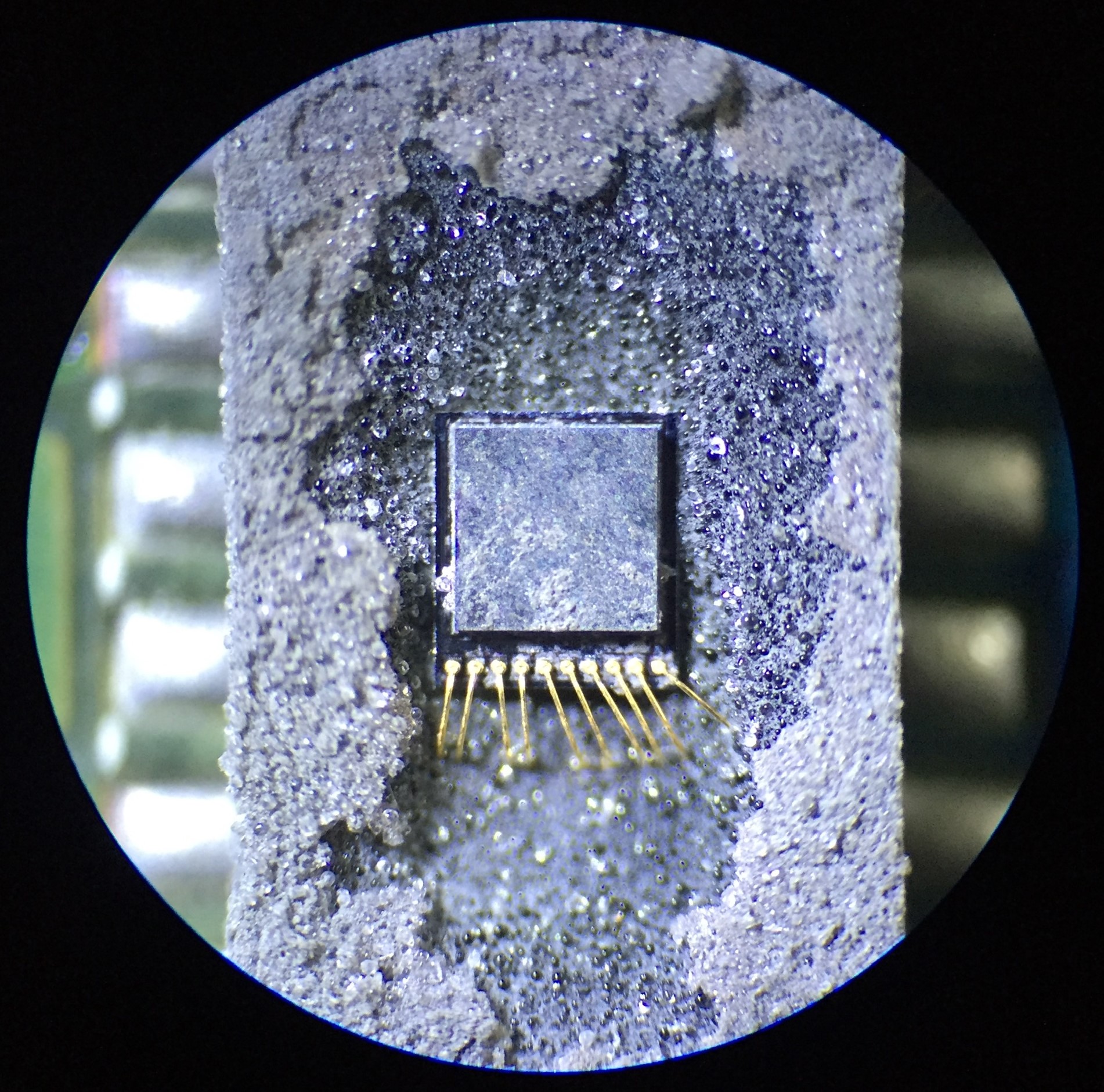
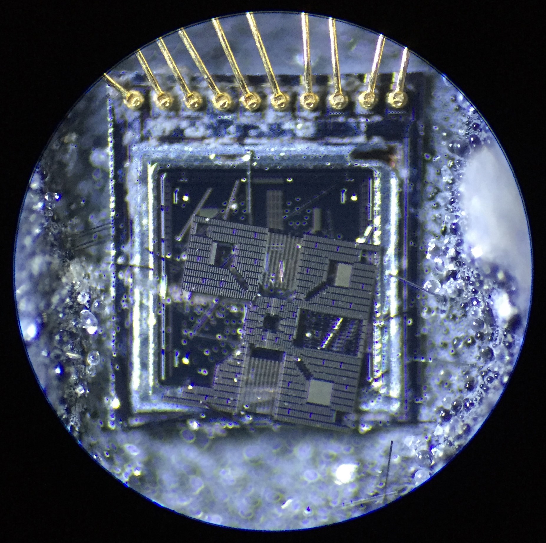
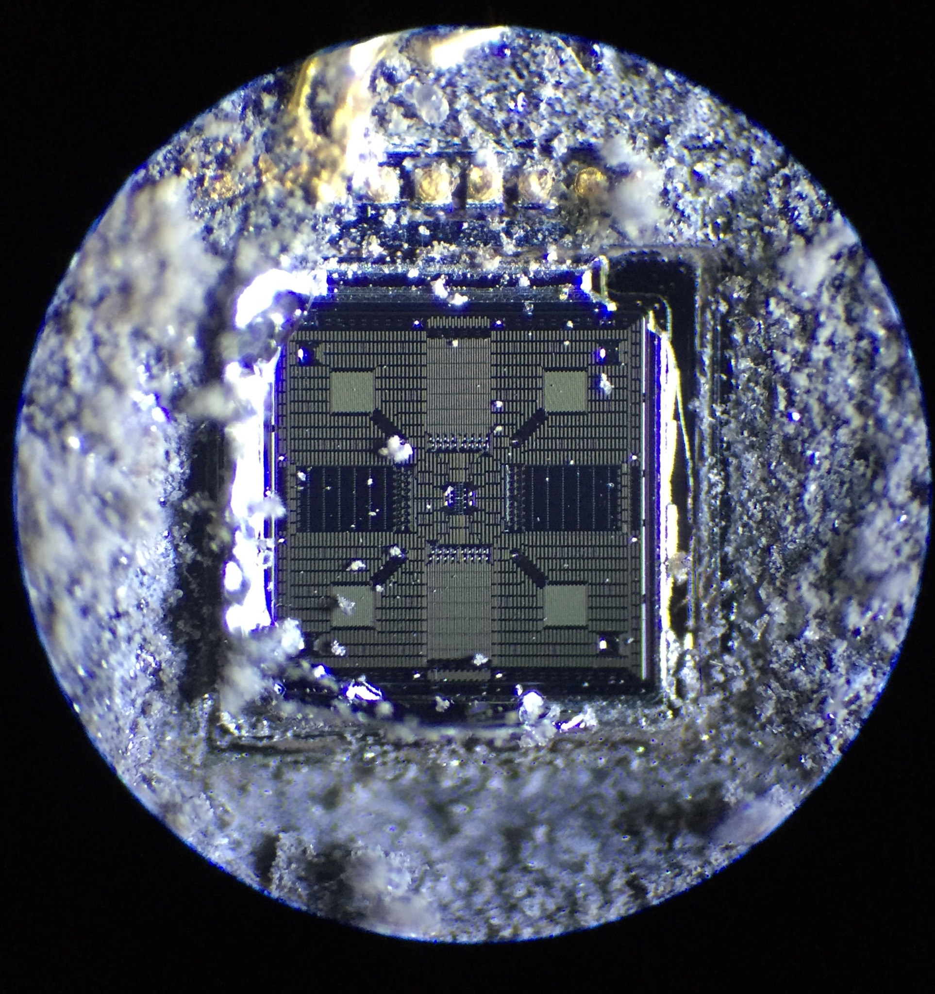

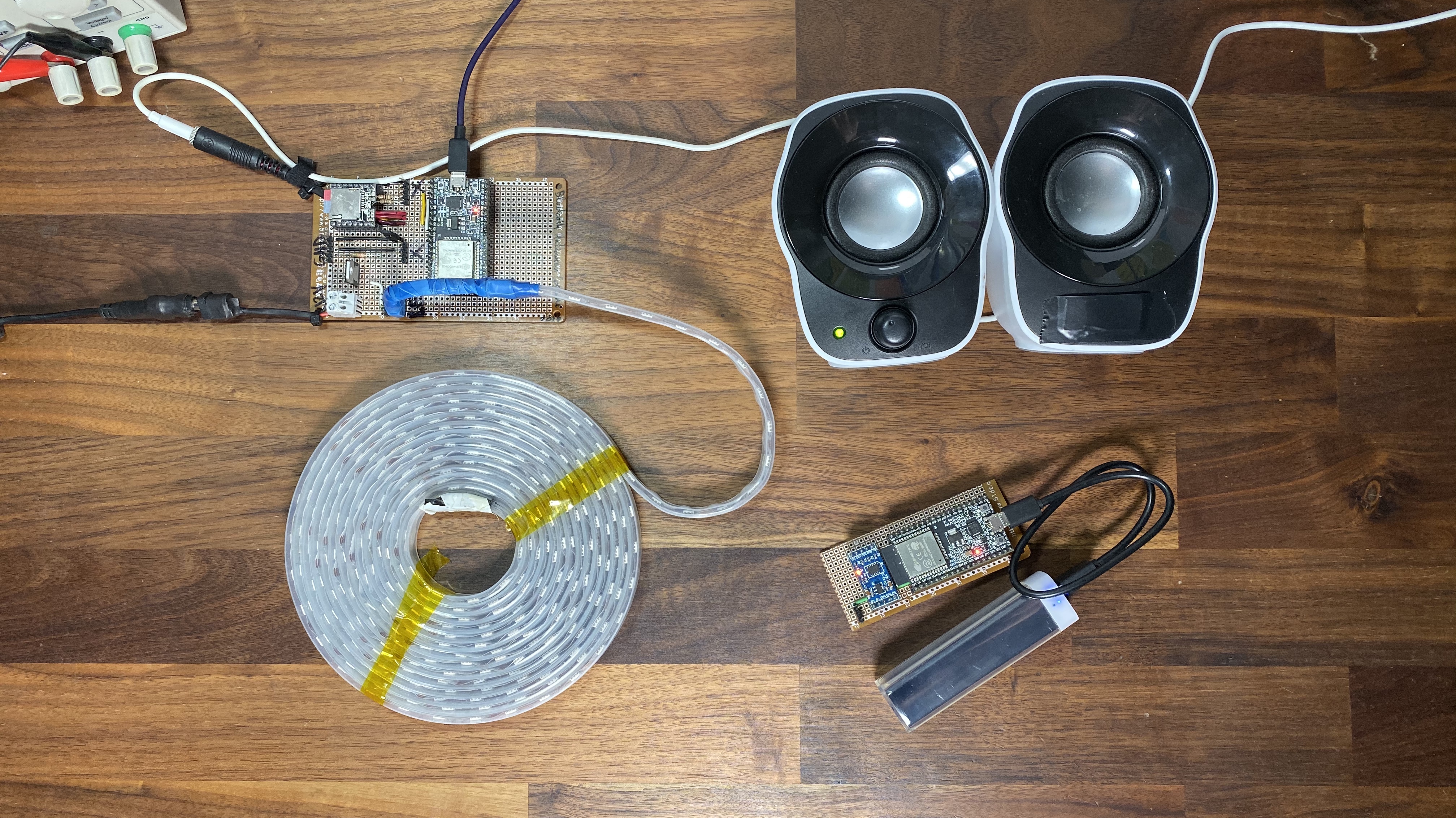
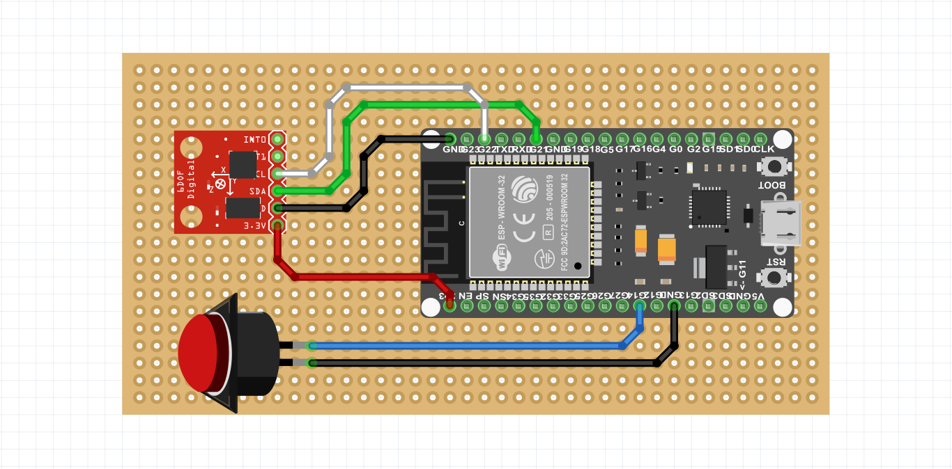
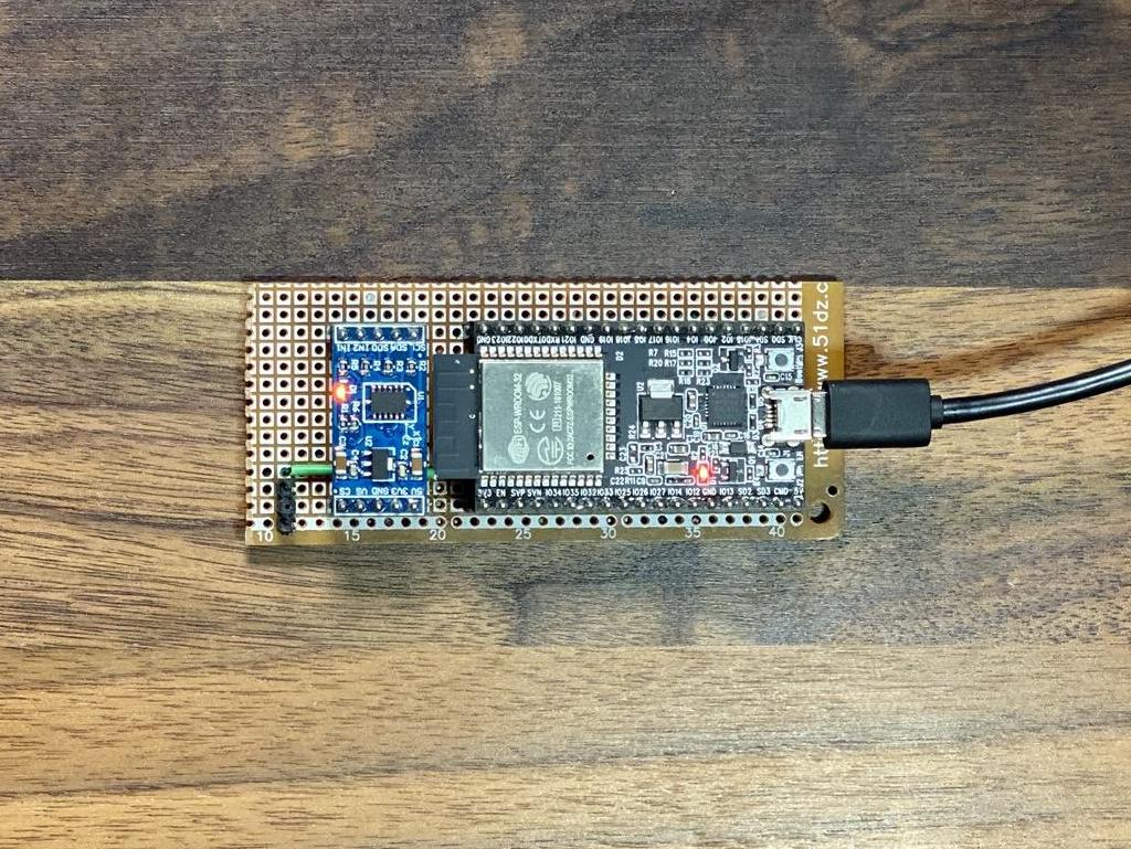
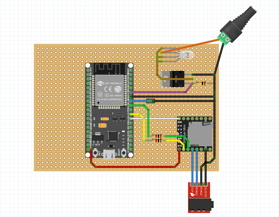
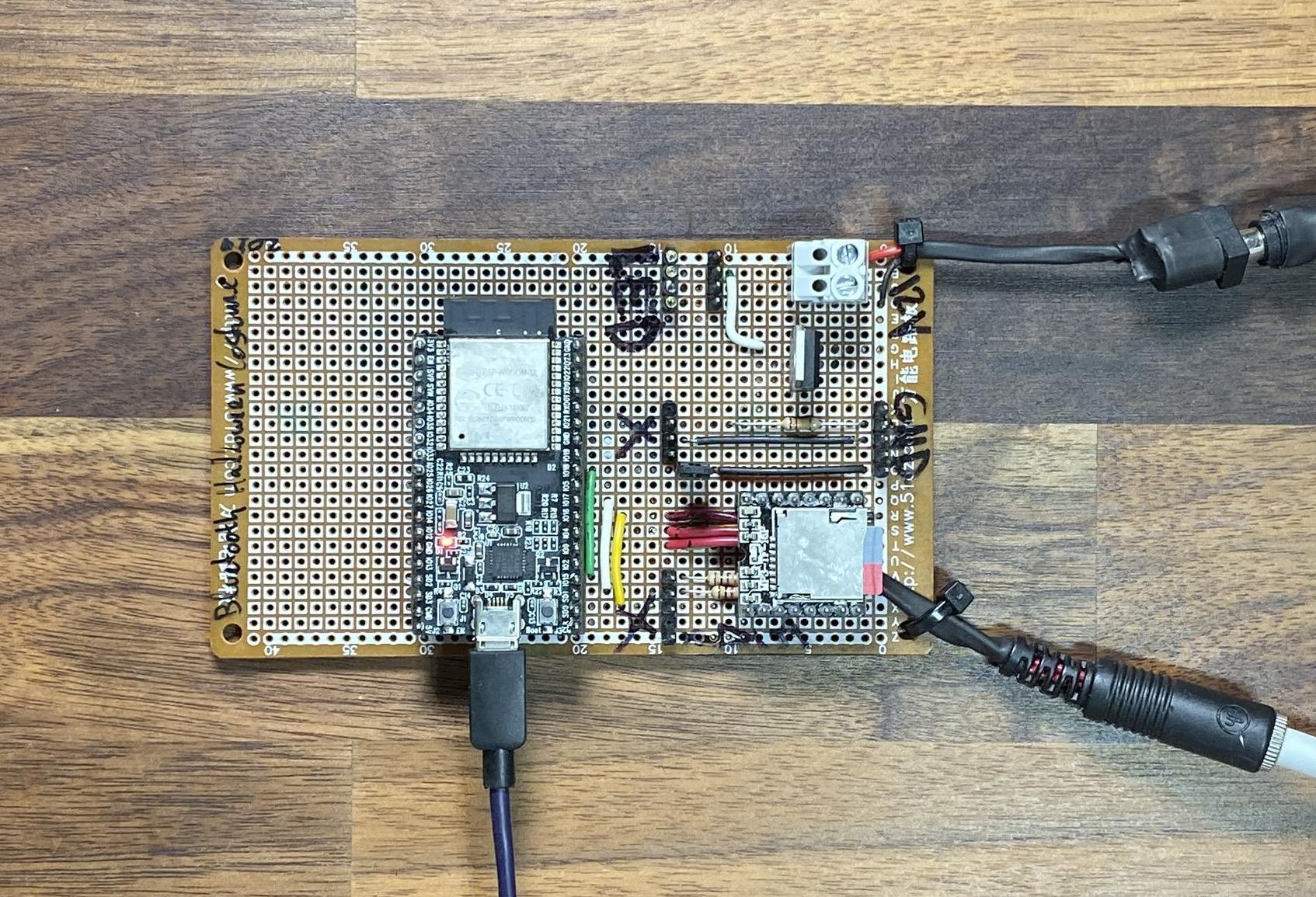
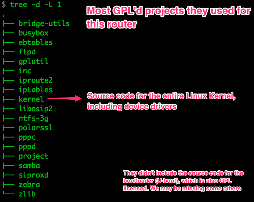
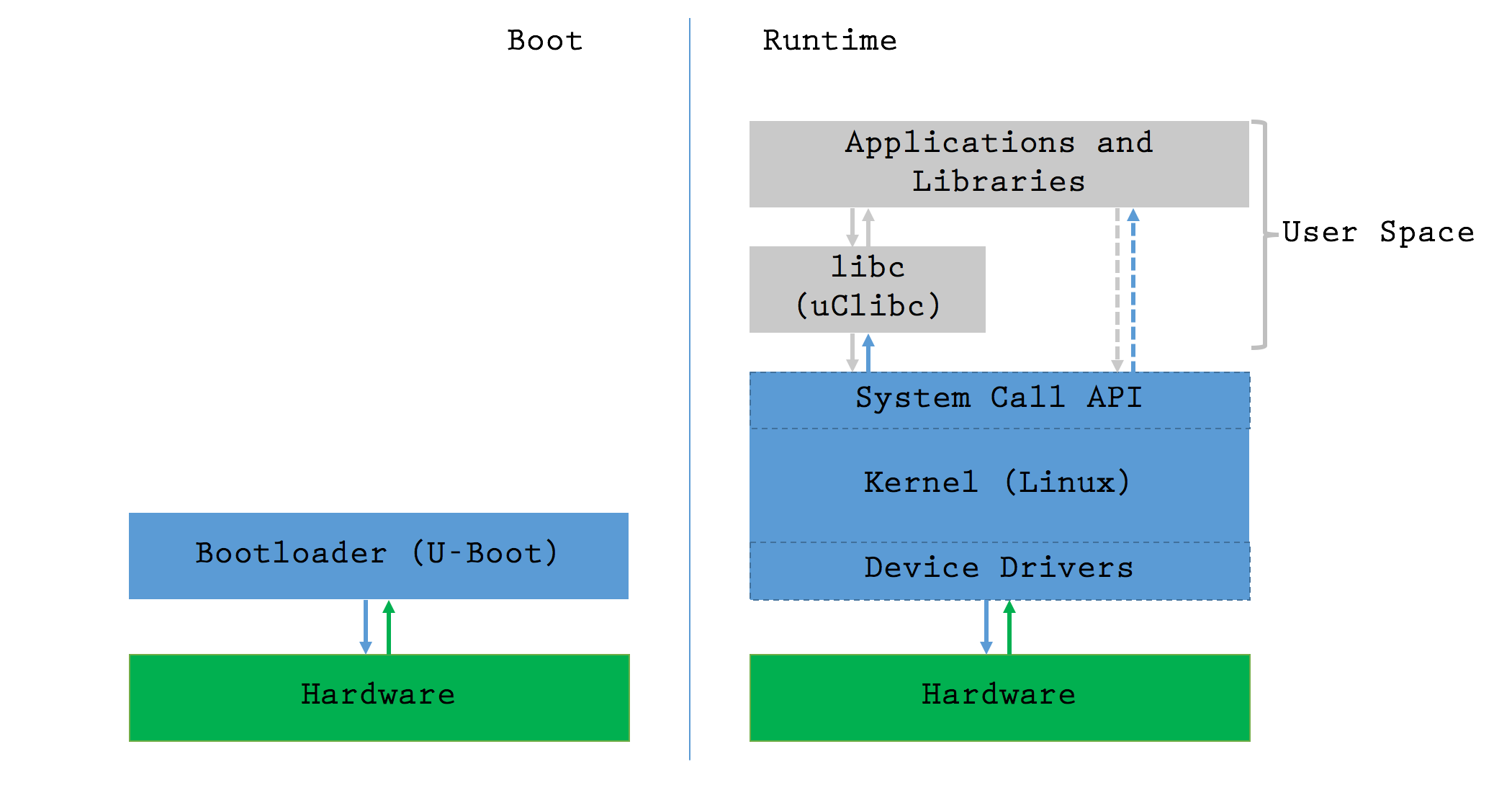
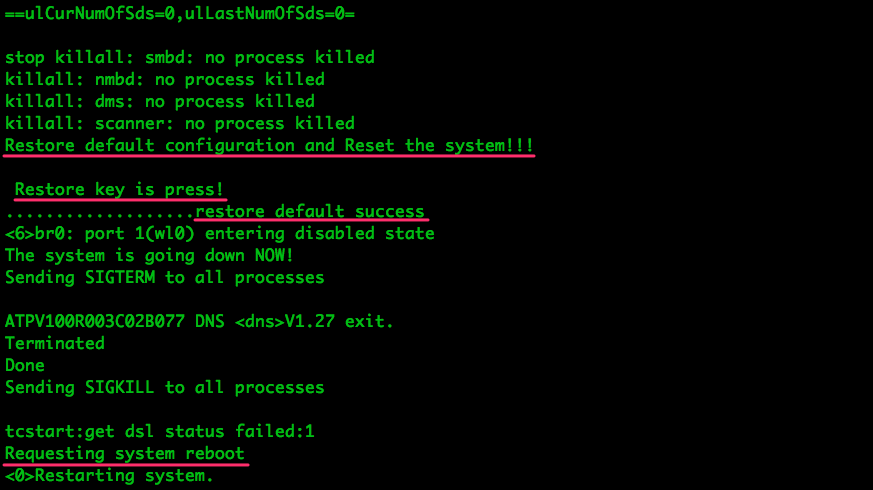
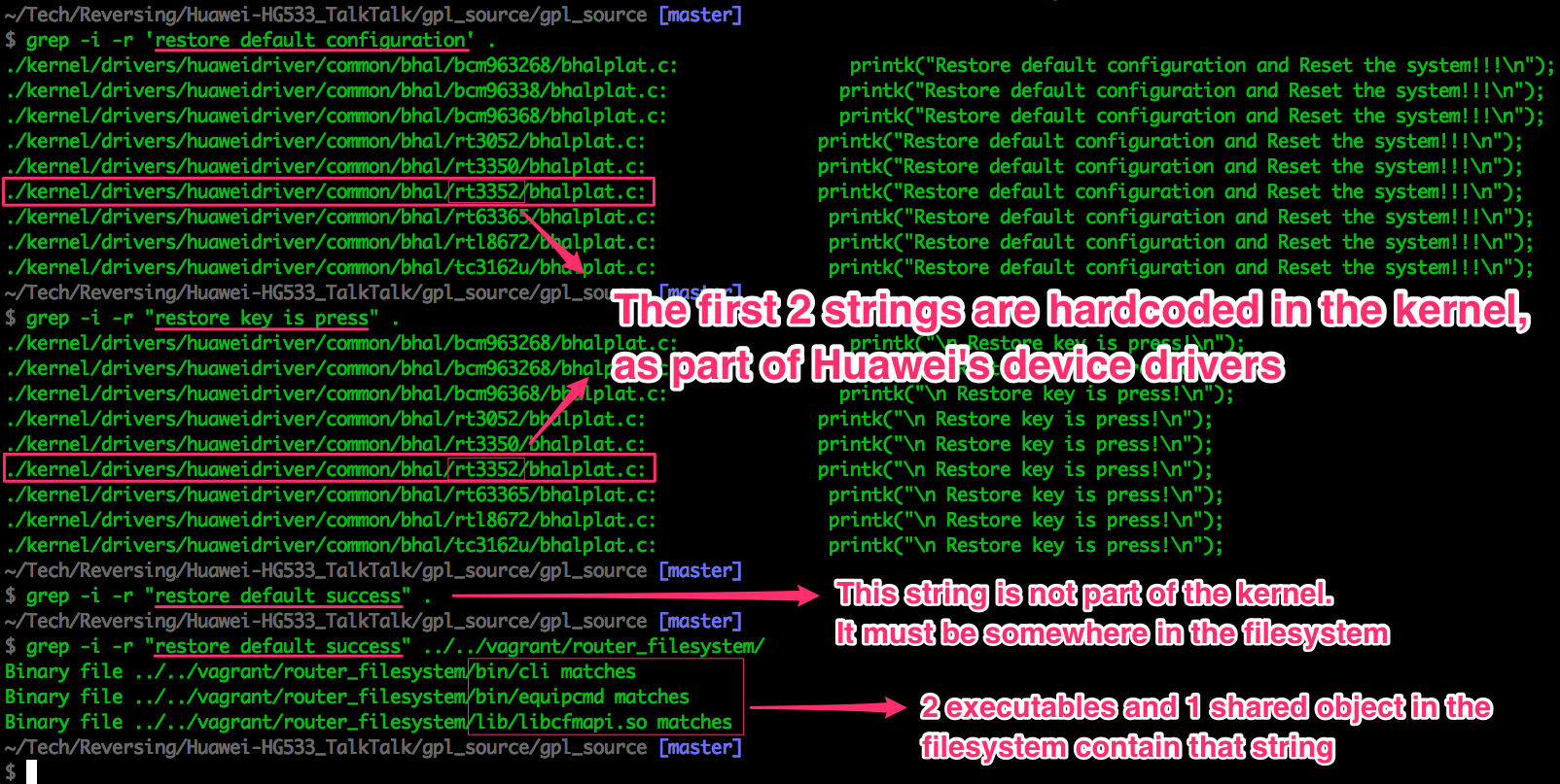
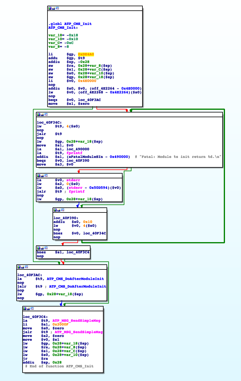
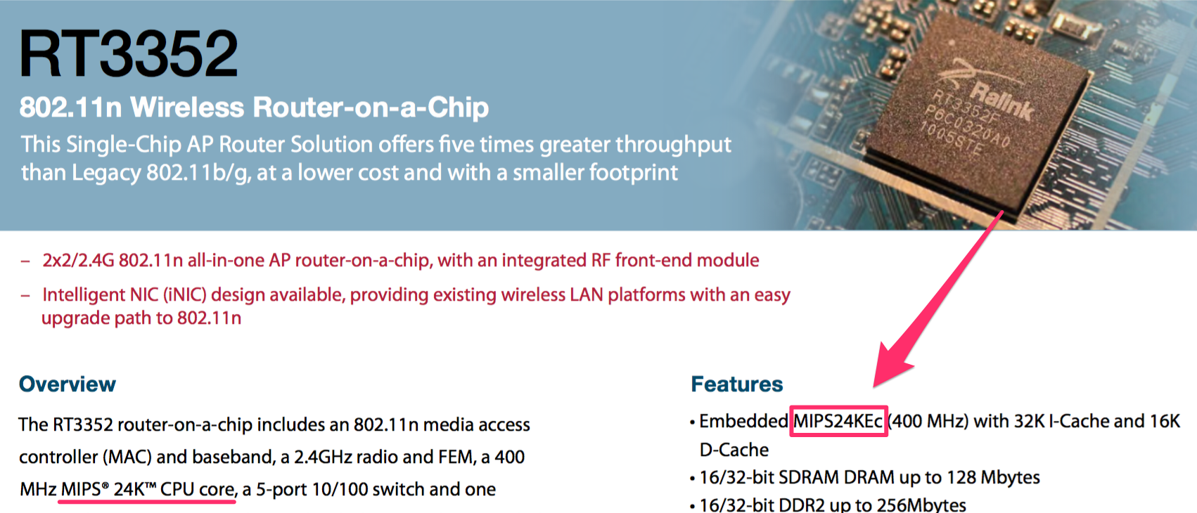
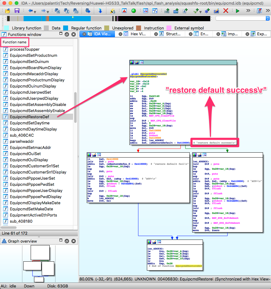
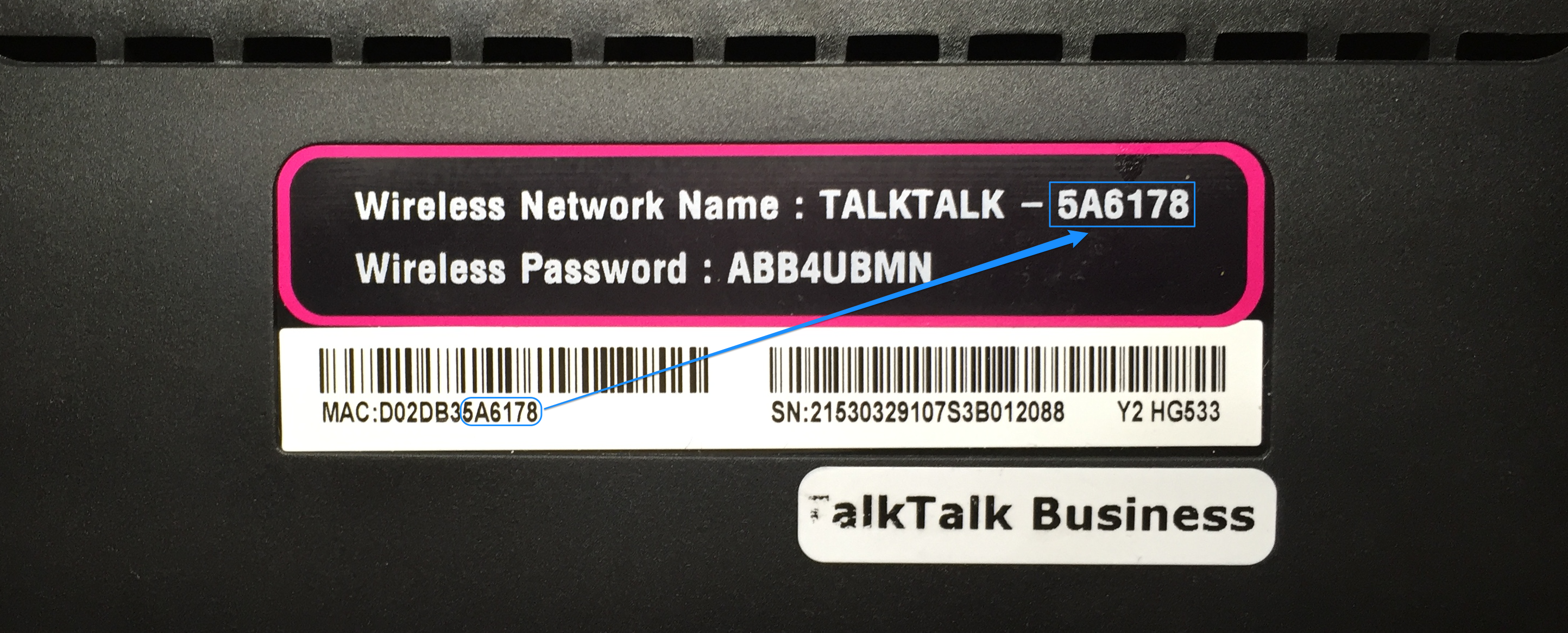
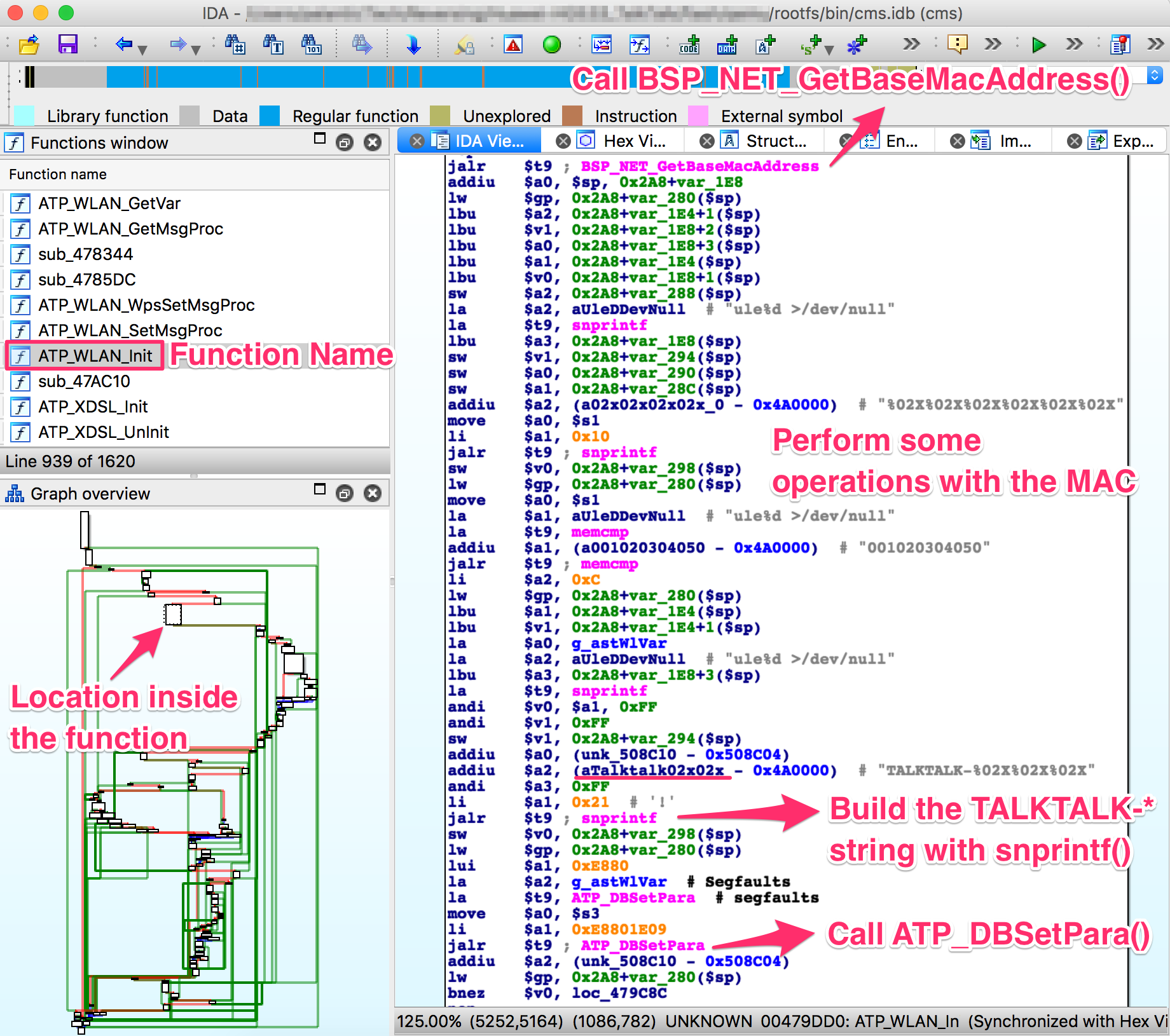
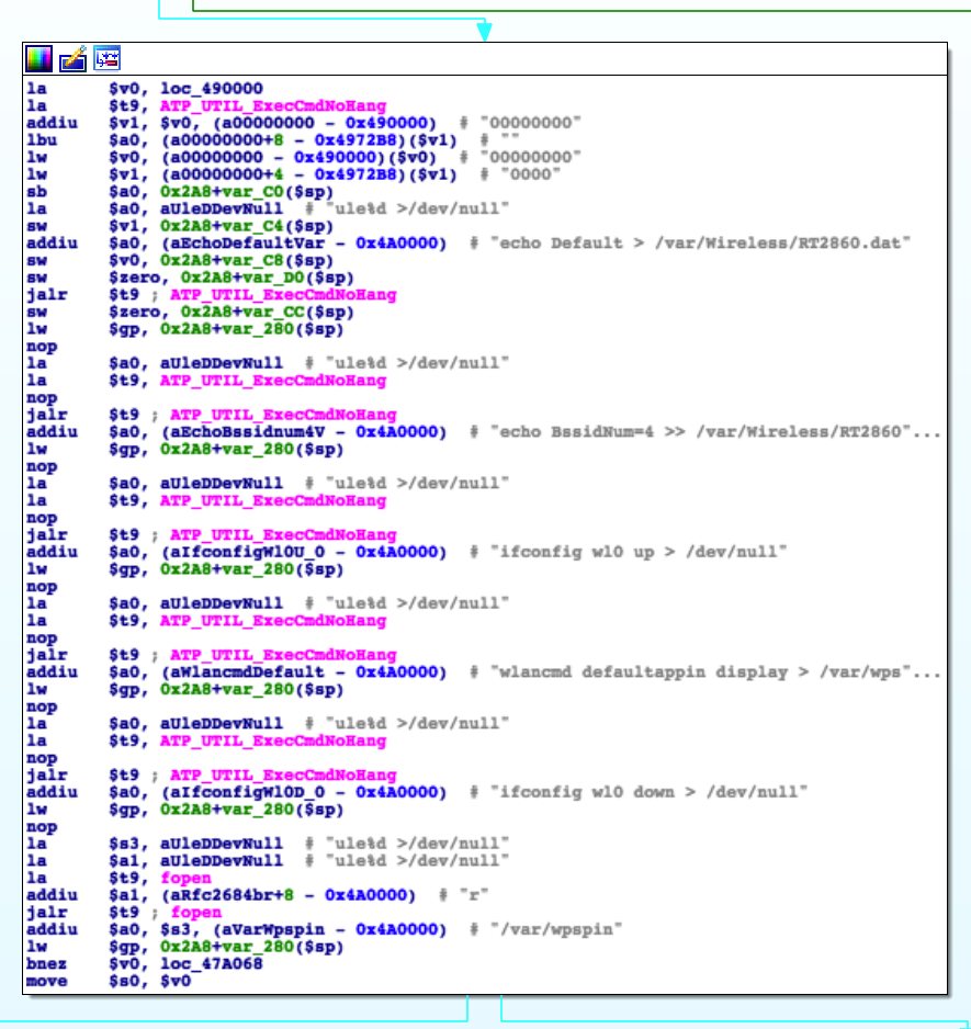
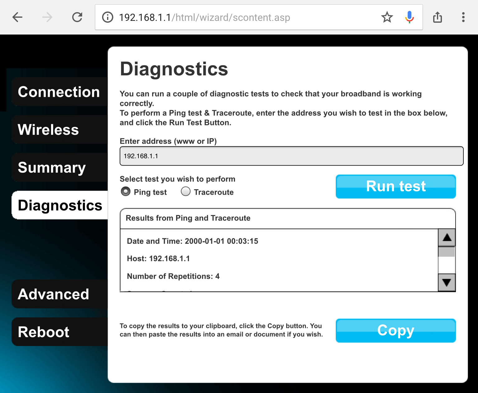
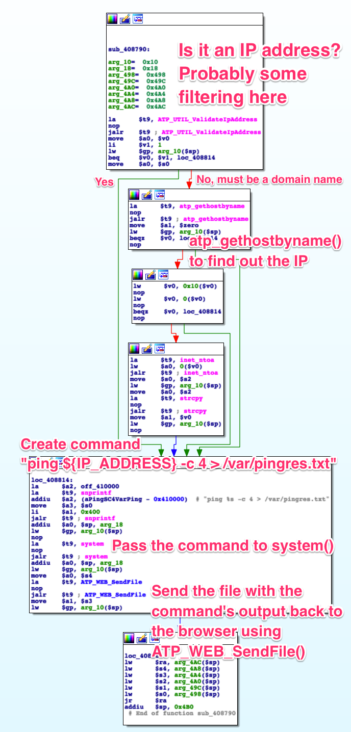
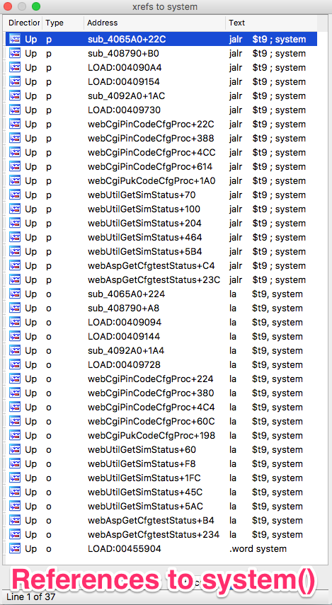
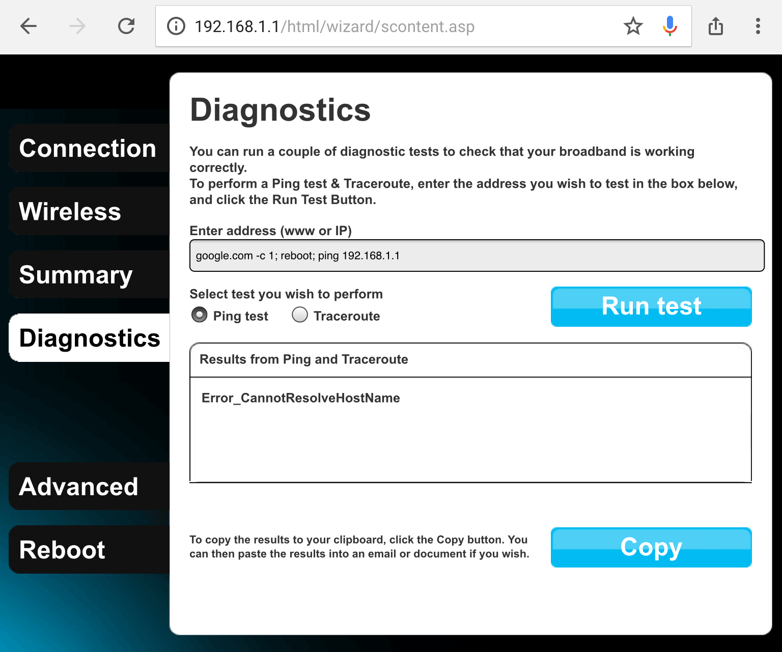
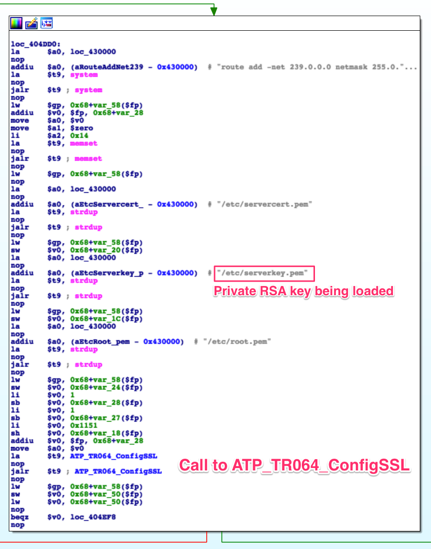
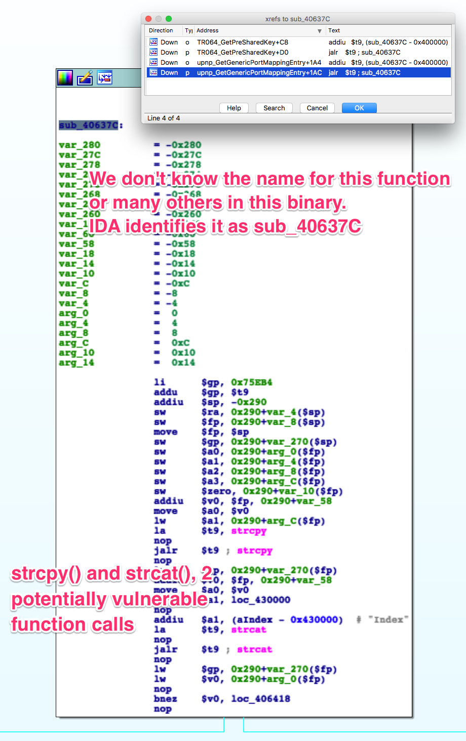
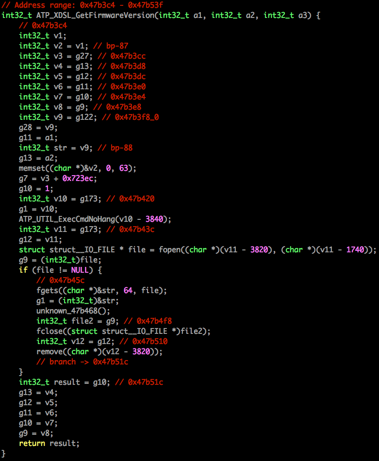