Practical Reverse Engineering Part 3 - Following the Data
23 May 2016- Part 1: Hunting for Debug Ports
- Part 2: Scouting the Firmware
- Part 3: Following the Data
- Part 4: Dumping the Flash
- Part 5: Digging Through the Firmware
The best thing about hardware hacking is having full access to very bare metal, and all the electrical signals that make the system work. With ingenuity and access to the right equipment we should be able to obtain any data we want. From simply sniffing traffic with a cheap logic analyser to using thousands of dollars worth of equipment to obtain private keys by measuring the power consumed by the device with enough precision (power analysis side channel attack); if the physics make sense, it’s likely to work given the right circumstances.
In this post I’d like to discuss traffic sniffing and how we can use it to gather intel.
Traffic sniffing at a practical level is used all the time for all sorts of purposes, from regular debugging during the delopment process to reversing the interface of gaming controllers, etc. It’s definitely worth a post of its own, even though this device can be reversed without it.
Please check out the legal disclaimer in case I come across anything sensitive.
Full disclosure: I’m in contact with Huawei’s security team. I tried to contact TalkTalk, but their security staff is nowhere to be seen.
Data Flows In the PCB
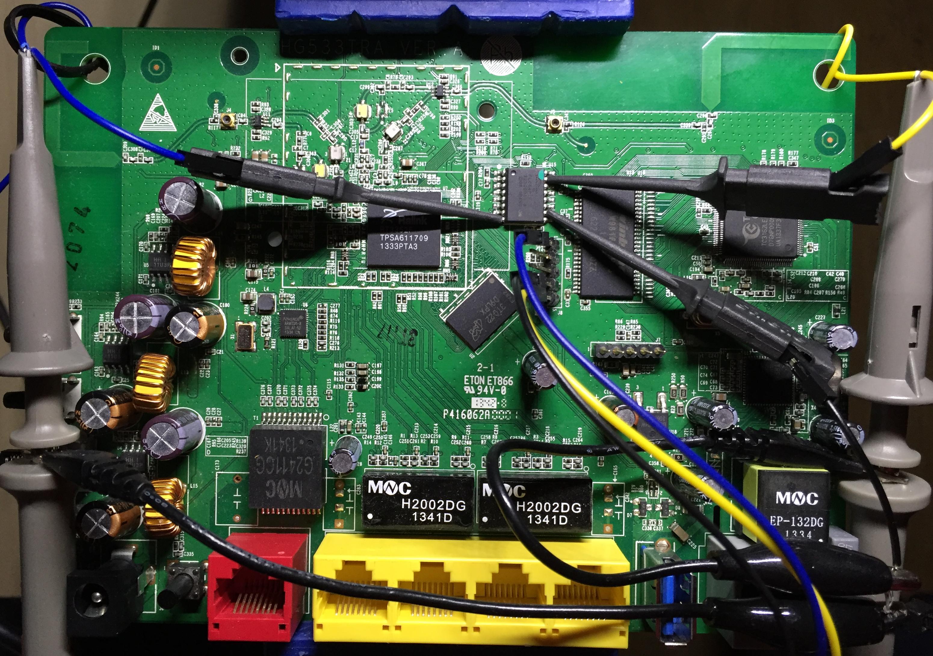
Data is useless within its static memory cells, it needs to be read, written and passed around in order to be useful. A quick look at the board is enough to deduce where the data is flowing through, based on IC placement and PCB traces:
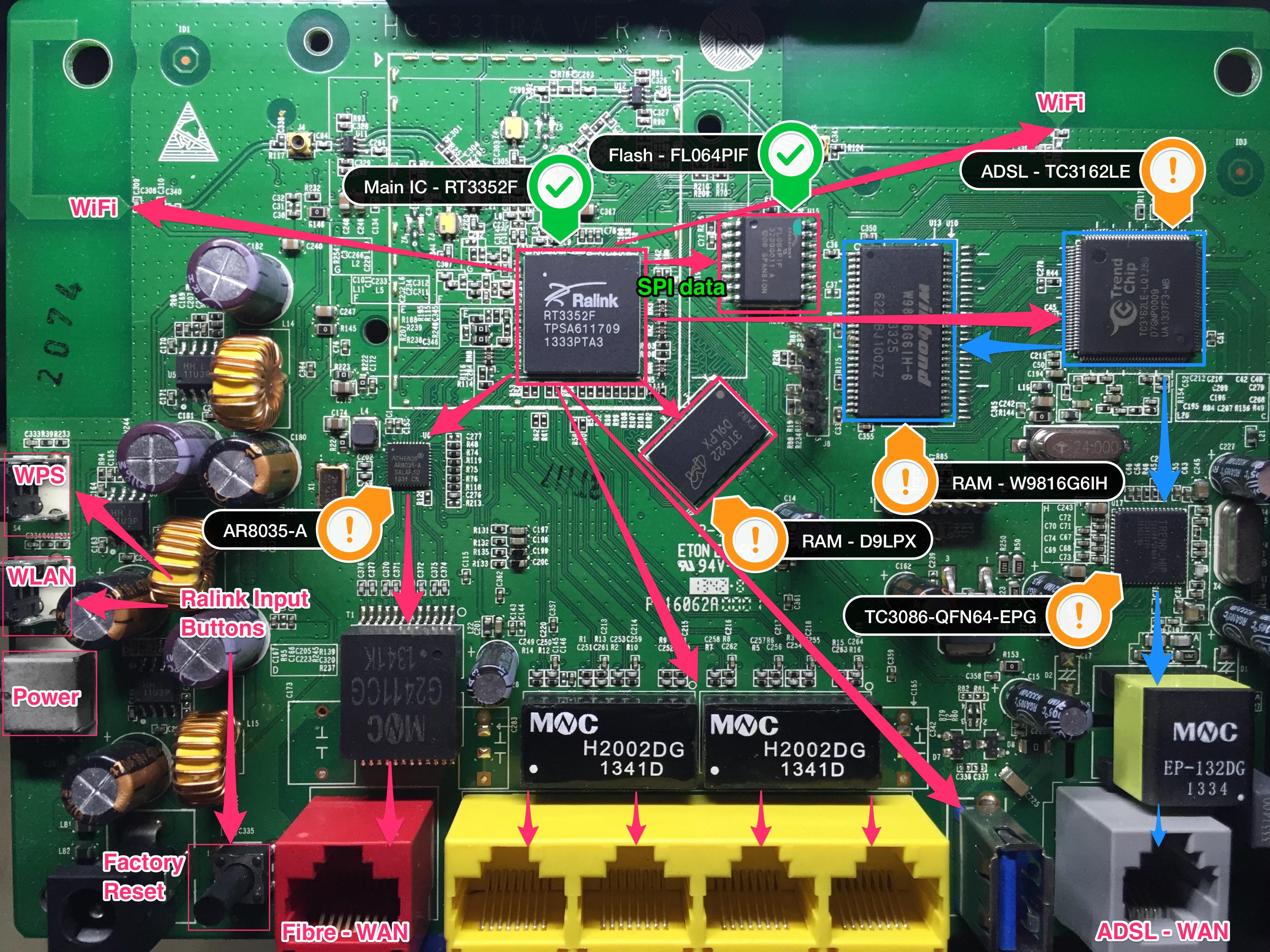
We’re not looking for hardware backdoors or anything buried too deep, so we’re only gonna look into the SPI data flowing between the Ralink and its external Flash.
Pretty much every IC in the market has a datasheet documenting all its technical characteristics, from pinouts to power usage and communication protocols. There are tons of public datasheets on google, so find the ones relevant to the traffic you want to sniff:
- Ralink RT3352F product brief: Not a datasheet, but it’s got some useful data
- Spansion FL064PIF: 64-Mbit SPI Flash Memory
Now we’ve got pinouts, electrical characteristics, protocol details… Let’s take a first look and extract the most relevant pieces of data.
Understanding the Flash IC
We know which data flow we’re interested: The SPI traffic between the Ralink IC and Flash. Let’s get started; the first thing we need is to figure out how to connect the logic analyser. In this case we’ve got the datasheet for the Flash IC, so there’s no need to reverse engineer any pinouts:
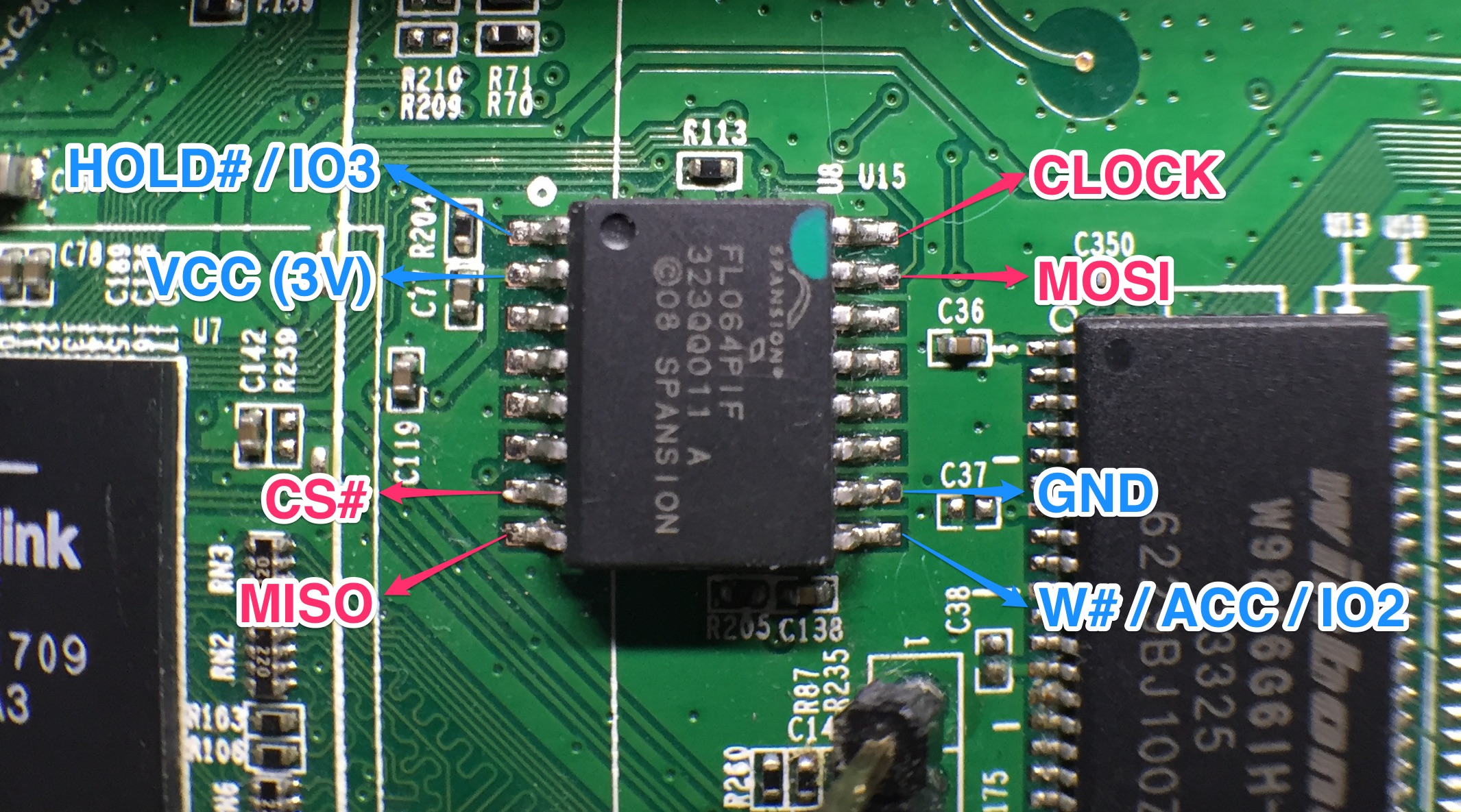
Standard SPI communication uses 4 pins:
- MISO (Master In Slave Out): Data line
Ralink<-Flash - MOSI (Master Out Slave In): Data line
Ralink->Flash - SCK (Clock Signal): Coordinates when to read the data lines
- CS# (Chip Select): Enables the Flash IC when set to
0so multiple of them can share MISO/MOSI/SCK lines.
We know the pinout, so let’s just connect a logic analyser to those 4 pins and capture some random transmission:
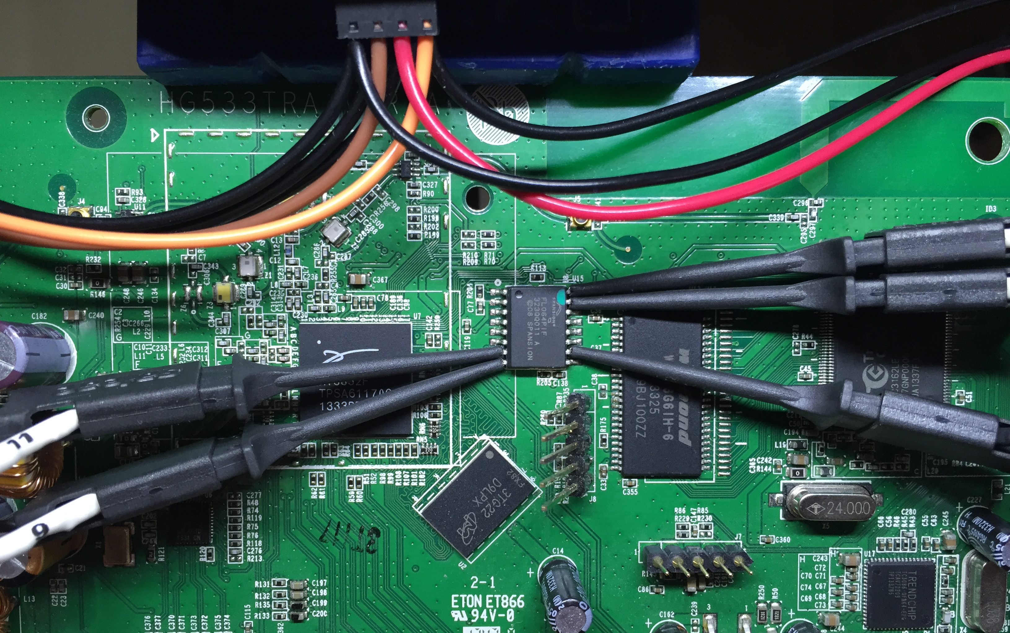
In order to set up our logic analyser we need to find out some SPI configuation options, specifically:
- Transmission endianness [Standard: MSB First]
- Number of bits per transfer [Standard: 8]. Will be obvious in the capture
- CPOL: Default state of the clock line while inactive [0 or 1]. Will be obvious in the capture
- CPHA: Clock edge that triggers the data read in the data lines [0=leading, 1=trailing]. We’ll have to deduce this
The datasheet explains that the flash IC understands only 2 combinations of CPOL and CPHA: (CPOL=0, CPHA=0) or (CPOL=1, CPHA=1)

Let’s take a first look at some sniffed data:

In order to understand exactly what’s happenning you’ll need the FL064PIF’s instruction set, available in its datasheet:
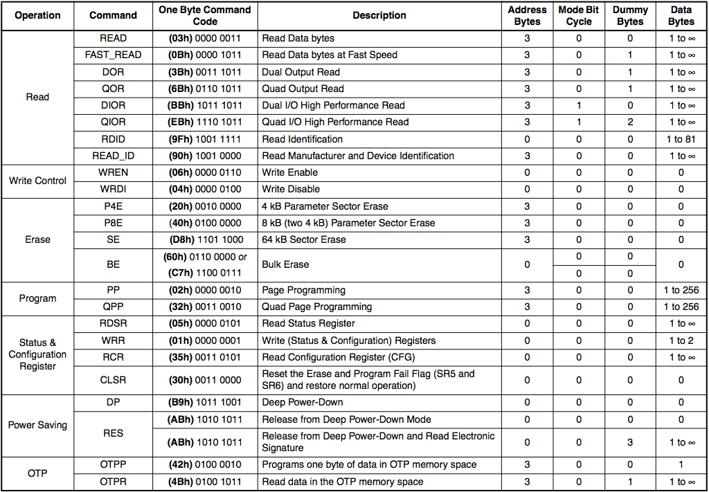
Now we can finally analyse the captured data:

In the datasheet we can see that the FL064PIF has high-performance features for read and write operations: Dual and Quad options that multiplex the data over more lines to increase the transmission speed. From taking a few samples, it doesn’t seem like the router uses these features much -if at all-, but it’s important to keep the possibility in mind in case we see something odd in a capture.
Transmission modes that require additional pins can be a problem if your logic analyser is not powerful enough.
The Importance of Your Sampling Rate [Theory]
A logic analyser is a conceptually simple device: It reads signal lines as
digital inputs every x microseconds for y seconds, and when it’s done it
sends the data to your computer to be analysed.
For the protocol analyser to generate accurate data it’s vital that we record digital inputs faster than the device writes them. Otherwise the data will be mangled by missing bits or deformed waveforms.
Unfortunately, your logic analyser’s maximum sampling rate depends on how powerful/expensive it is and how many lines you need to sniff at a time. High-speed interfaces with multiple data lines can be a problem if you don’t have access to expensive equipment.
I recorded this data from the Ralink-Flash SPI bus using a low-end Saleae
analyser at its maximum sampling rate for this number of lines,
24 MS/s:

As you can see, even though the clock signal has the 8 low to high transitions required for each byte, the waveform is deformed.
Since the clock signal is used to coordinate when to read the data lines, this kind of waveform deformation may cause data corruption even if we don’t drop any bits (depending partly on the design of your logic analyser). There’s always some wiggle room for read inaccuracies, and we don’t need 100% correct data at this point, but it’s important to keep all error vectors in mind.
Let’s sniff the same bus using a higher performance logic analyser at
100 MS/s:

As you can see, this clock signal is perfectly regular when our Sampling Rate is high enough.
If you see anything dodgy in your traffic capture, consider how much data you’re willing to lose and whether you’re being limited by your equipment. If that’s the case, either skip this Reversing vector or consider investing in a better logic analyser.
Seeing the Data Flow
We’re already familiar with the system thanks to the overview of the firmware we did in Part 2, so we can think of some specific SPI transmissions that we may be interested in sniffing. Simply connecting an oscilloscope to the MISO and MOSI pins will help us figure out how to trigger those transmissions and yield some other useful data.
Here’s a video (no audio) showing both the serial interface and the MISO/MOSI signals while we manipulate the router:
This is a great way of easily identifying processes or actions that trigger flash read/write actions, and will help us find out when to start recording with the logic analyser and for how long.
Analysing SPI Traffic - ATP’s Save Command
In Post 2 I mentioned ATP CLI has a save command that stores something to
flash; unfortunately, the help menu (save ?) won’t tell you what it’s doing
and the only output when you run it is a few dots that act as a progress bar.
Why don’t we find out by ourselves? Let’s make a plan:
- Wait until boot sequence is complete and the router is idle so there’s no unexpected SPI traffic
- Start the
ATP Clias explained in Part 1 - Connect the oscilloscope to MISO/MOSI and run
saveto get a rough estimate of how much time we need to capture data for - Set a trigger in the
enableline sniffed by the logic analyser so it starts recording as soon as the flash IC is selected - Run
save - Analyse the captured data
Steps 3 and 4 can be combined so you see the data flow in real time in the scope while you see the charge bar for the logic analyser; that way you can make sure you don’t miss any data. In order to comfortably connect both scope and logic sniffer to the same pins, these test clips come in very handy:
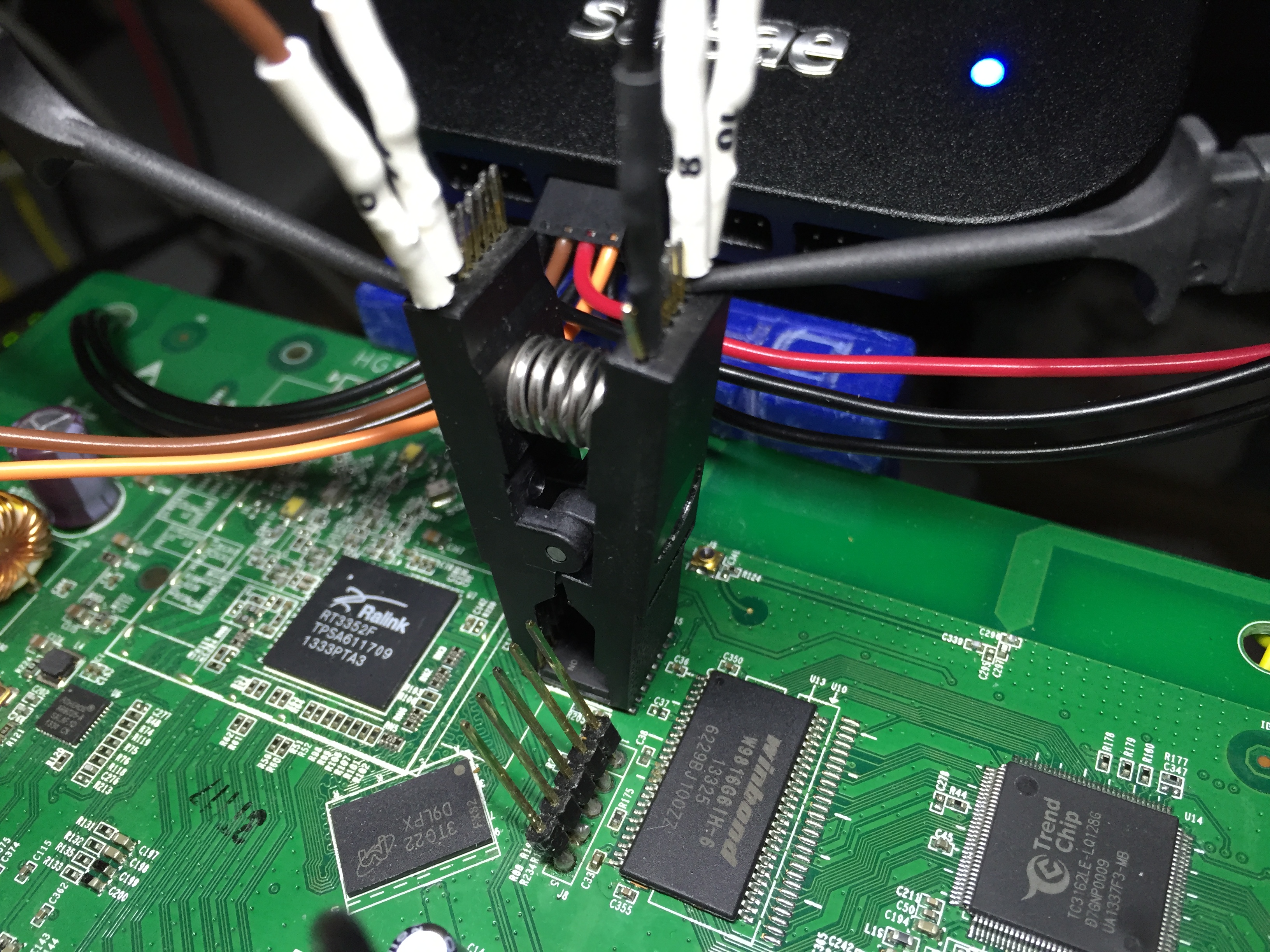
Once we’ve got the traffic we can take a first look at it:

Let’s consider what sort of data could be extracted from this traffic dump that might be useful to us. We’re working with a memory storage IC, so we can see the data that is being read/written and the addresses where it belongs. I think we can represent that data in a useful way by 2 means:
- Traffic map depicting which Flash areas are being written, read or erased in chronological order
- Create binary files that replicate the memory blocks that were read/written, preferably removing all the protocol rubbish that we sniffed along with them.
Saleae’s SPI analyser will export the data as a CSV file. Ideally we’d improve their protocol analyser to add the functionality we want, but that would be too much work for this project. One of the great things about low level protocols like SPI is that they’re usually very straightforward; I decided to write some python spaghetti code to analyse the CSV file and extract the data we’re looking for: binmaker.py and traffic_mapper.py
The workflow to analyse a capture is the following:
- Export sniffed traffic as CSV
- Run the script:
- Iterate through the CSV file
- Identify different commands by their index
- Recognise the command expressed by the first byte
- Process its arguments (addresses, etc.)
- Identify the read/write payload
- Convert ASCII representation of each payload byte to binary
- Write binary blocks to different files for MISO (read) and MOSI (write)
- Read the traffic map (regular text) and the binaries
(
hexdump -C output.bin | less)
The scripts generate these results:
- Traffic Map
- Replicated Memory Blocks, Merged: MOSI and MISO
- Replicated Memory Blocks, Split by address: Files list
The traffic map is much more useful when combined with the Flash memory map we found in Part 2:

From the traffic map we can see the bulk of the save command’s traffic is
simple:
- Read about 64kB of data from the
protectarea - Overwrite the data we just read
In the MISO binary we can see most of the read data was just tons of 1s:

Most of the data in the MOSI binary is plaintext XML, and it looks exactly like
the /var/curcfg.xml file we discovered in Part 2. As we discussed then, this
“current configuration” file contains tons of useful data, including the current
WiFi credentials.
It’s standard to keep reserved areas in flash; they’re mostly for
miscellaneous data that needs to survive across reboots and be configurable
by user, firmware or factory. It makes sense for a command called save to
write data to such area, it explains why the data is perfectly readable as
opposed to being compressed like the filesystem, and why we found the XML file
in the /var/ folder of the filesystem (it’s a folder for runtime files; data in
the protect area has to be loaded to memory separately from the filesystem).
The Pot of Gold at the End of the Firmware [Theory]
During this whole process it’s useful to have some sort of target to keep you digging in the same general direction.
Our target is an old one: the algorithm that generates the router’s default WiFi password. If we get our hands on such algorithm and it happens to derive the password from public information, any HG533 in the world with default WiFi credentials would probably be vulnerable.
That exact security issue has been found countless times in the past, usually deriving the password from public data like the Access Point’s MAC address or its SSID.
That being said, not all routers are vulnerable, and I personally don’t expect this one to be. The main reason behind targeting this specific vector is that it’s caused by a recurrent problem in embedded engineering: The need for a piece of data that is known by the firmware, unique to each device and known by an external entity. From default WiFi passwords to device credentials for IoT devices, this problem manifests in different ways all over the Industry.
Future posts will probably reference the different possibilities I’m about to explain, so let me get all that theory out of the way now.
The Sticker Problem
In this day and era, connecting to your router via ethernet so there’s no need for default WiFi credentials is not an option, using a display to show a randomly generated password would be too expensive, etc. etc. etc. The most widely adopted solution for routers is to create a WiFi network using default credentials, print those credentials on a sticker at the factory and stick it to the back of the device.
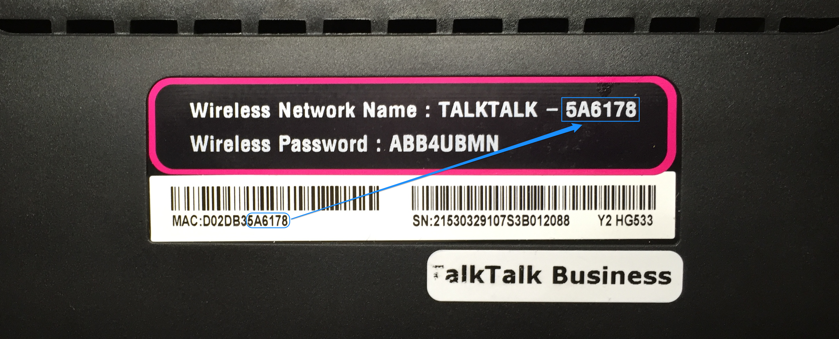
The WiFi password is the ‘unique piece of data’, and the computer printing the stickers in the factory is the ‘external entity’. Both the firmware and the computer need to know the default WiFi credentials, so the engineer needs to decide how to coordinate them. Usually there are 2 options available:
- The same algorithm is implemented in both the device and the computer, and its input parameters are known to both of them
- A computer generates the credentials for each device and they’re stored into each device separately
Developer incompetence aside, the first approach is usually taken as a last resort; if you can’t get your hardware manufacturer to flash unique data to each device or can’t afford the increase in manufacturing cost.
The second approach is much better by design: We’re not trusting the hardware with data sensitive enough to compromise every other device in the field. That being said, the company may still decide to use an algorithm with predictable outputs instead of completely random data; that would make the system as secure as the weakest link between the algorithm -mathematically speaking-, the confidentiality of their source code and the security of the computers/network running it.
Sniffing Factory Reset
So now that we’ve discussed our target, let’s gather some data about it. The first thing we wanna figure out is which actions will kickstart the flow of relevant data on the PCB. In this case there’s 1 particular action: Pressing the Factory Reset button for 10s. This should replace the existing WiFi credentials with the default ones, so the default creds will have to be generated/read. If the key or the generation algorithm need to be retrieved from Flash, we’ll see them in a traffic capture.
That’s exactly what we’re gonna do, and we’re gonna observe the UART interface,
the oscilloscope and the logic analyser during/after pressing the reset button.
The same process we followed for ATP’s save gives us these results:
UART output:
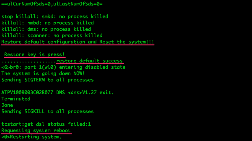
Traffic overview:

Output from our python scripts:
The traffic map tells us the device first reads and overwrites 2 large chunks
of data from the protect area and then reads a smaller chunk of data from the
filesystem (possibly part of the next process to execute):
___________________
|Transmission  Map|
|  MOSI  |  MISO  |
|        |0x7e0000| Size: 12    //Part of the Protected area
|        |0x7e0000| Size: 1782
|        |0x7e073d| Size: 63683
| ERASE 0x7e073d  | Size: 64kB
|0x7e073d|        | Size: 195
|0x7e0800|        | Size: 256
|0x7e0900|        | Size: 256
---------//--------
       [...]
---------//--------
|0x7e0600|        | Size: 256
|0x7e0700|        | Size: 61
|        |0x7d0008| Size: 65529 //Part of the Protected area
| ERASE 0x7d0008  | Size: 64kB
|0x7d0008|        | Size: 248
|0x7d0100|        | Size: 256
---------//--------
       [...]
---------//--------
|0x7dff00|        | Size: 256
|0x7d0000|        | Size: 8
|        |0x1c3800| Size: 512   //Part of the Filesystem
|        |0x1c3a00| Size: 512
---------//--------
       [...]
---------//--------
|        |0x1c5a00| Size: 512
|        |0x1c5c00| Size: 512
-------------------
Once again, we combine transmission map and binary files to gain some insight into the system. In this case, the ‘factory reset’ code seems to:
- Read
ATP_LOGfrom Flash; it contains info such as remote router accesses or factory resets. It ends with a large chunk of1s (0xff) - Overwrite that memory segment with
1s - write a ‘new’
ATP_LOGfollowed by the “current configuration”curcfg.xmlfile - Read compressed (unintelligible to us) memory chunk from the filesystem
The chunk from the filesystem is read AFTER writing the new password to Flash, which doesn’t make sense for a password generation algorithm. That being said, the algorithm may be already loaded into memory, so its absence in the SPI traffic is not conclusive on whether or not it exists.
As part of the MOSI data we can see the new WiFi password be saved to Flash inside the XML string:
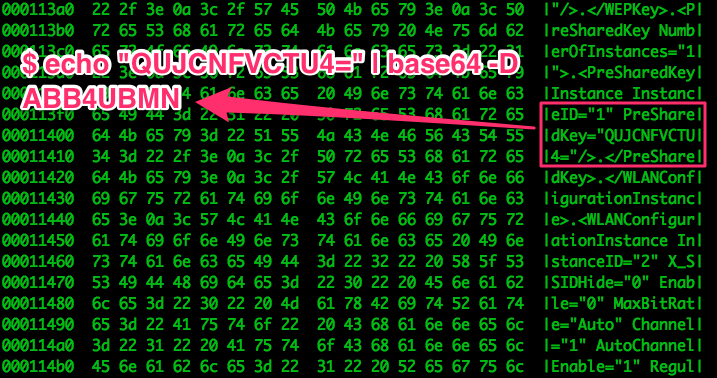
What about the default password being read? If we look in the MISO binary, it’s nowhere to be seen. Either the Ralink is reading it using a different mode (secure/dual/quad/?) or the credentials/algorithm are already loaded in RAM (no need to read them from Flash again, since they can’t change). The later seems more likely, so I’m not gonna bother updating my scripts to support different read modes. We write down what we’ve found and we’ll get back to the default credentials in the next part.
Since we’re at it, let’s take a look at the SPI traffic generated when setting
new WiFi credentials via HTTP:
Map,
MISO,
MOSI.
We can actually see the default credentials being read from the protect area
of Flash this time (not sure why the Ralink would load it to set a new
password; it’s probably incidental):
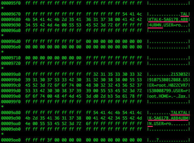
As you can see, they’re in plain text and separated from almost anything else in Flash. This may very well mean there’s no password generation algorithm in this device, but it is NOT conclusive. The developers could have decided to generate the credentials only once (first boot?) and store them to flash in order to limit the number of times the algorithm is accessed/executed, which helps hide the binary that contains it. Otherwise we could just observe the running processes in the router while we press the Factory Reset button and see which ones spawn or start consuming more resources.
Next Steps
Now that we’ve got the code we need to create binary recreations of the traffic and transmission maps, getting from a capture to binary files takes seconds. I captured other transmissions such as the first few seconds of boot (map, miso), but there wasn’t much worth discussing. The ability to easily obtain such useful data will probably come in handy moving forward, though.
In the next post we get the data straight from the source, communicating with the Flash IC directly to dump its memory. We’ll deal with compression algorithms for the extracted data, and we’ll keep piecing everything together.
Happy Hacking! :)