Learning to Decapsulate Integrated Circuits Using Acid Deposition
20 Oct 2020In this post:
- Known decapping methodologies
- Personal safety
- My experiments
- Tools and materials
- Failure: Sand down the packaging
- Limited success: Nitric acid + acetone bath
- Failure: Nitric acid + acetone syringe
- Failure: Nitric acid + acetone syringe + ultrasonic methanol bath
- Success: Nitric acid + acetone syringe + ultrasonic acetone bath
- Pointless: Bath the IC in room-temp nitric acid before cleanup
- Success: Using a mix of Sulfuric and Nitric acids
- How I took the silicon die pictures
- Pretty pictures of silicon dies
- Resources
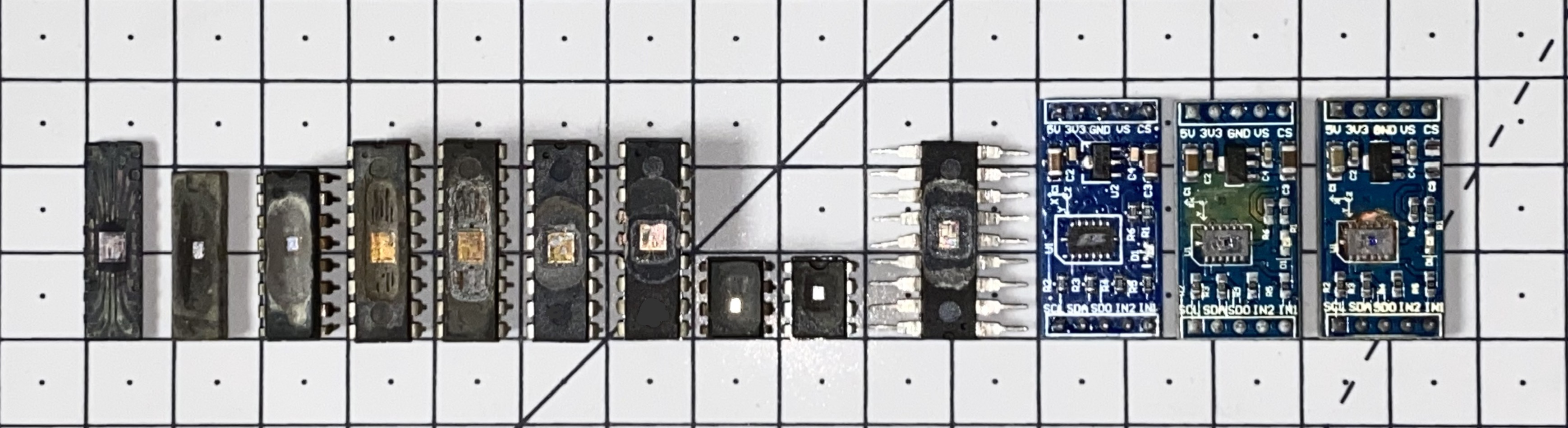
I’ve been looking to try my hand at IC decapsulation for years, and finally got the time to do it. The process took plenty of trial and error, so this post will document most of my failures and successes, and detail the methodologies used for each attempt. These are most of the ICs I worked on throughout the process:
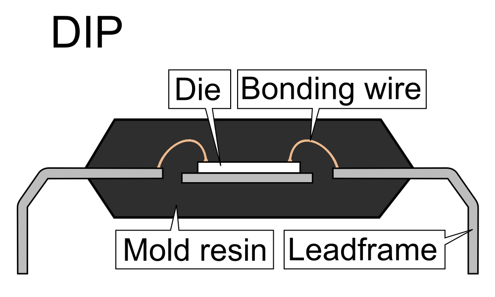
A typical chip is built as a silicon die, connected to its leads/contacts through bonding wires, and encapsulated in resin for protection.
Of course, there are other ICs that use different designs and encapsulation materials: mostly metal and plastics. But the epoxy-based design is extremely common, so we’ll be focusing on it.
This picture of a DIP package -courtesy of Wikipedia- explains it very well:
The decapsulation/decapping of Integrated Circuits, also known as “delidding”, is nothing new.
It’s used in the industry to debug hardware issues, reverse engineer chips, verify the authenticity of parts, and other tasks that require access to the underlying circuitry.
That’s why there’s plenty of commercial services that will decapsulate your ICs using expensive and dedicated equipment. I’ve linked a couple of them in the bibliography. But, without having any idea how much they cost or how long they take, I can’t imagine them being an option for the average hacker.
Hackers and smaller companies generally decap Integrated Circuits to identify counterfeits, gain a very rudimentary understanding of the parts comprising them, or just to share the pretty pictures of the silicon die. For those cases, a DIY process is generally good enough.
Decapping/delidding has also been used by hackers for more fun purposes, such as unsetting efuses from production hardware to extract and/or override their firmware, private keys, etc. So there are cases where a commercial-level result can be worth it.
I’ve been wanting to try my hand at decapping ICs for years, for no other purpose than to satiate my curiosity. I’ve finally had the time to get to it, so this post will describe the methods I tried and the hurdles I encountered.
Existing methodologies
The biggest factor to decide which method is best for your project is whether or not you need the chip to still work after it’s been decapsulated. That means not destroying or disconnecting the die, bonding wires, external contact points, etc. so you can still use the chip after the process is complete.
Here’s a list of the most common options.
Destructive methods:
- Burn the encapsulation to hell using a blowtorch
- Full wet chemical decapsulation: Bath the entire chip in acid to remove all encapsulation, leads, bonds, etc.
Non-destructive methods:
- Selective wet chemical decapsulation:
- Rubber gaskets + acid yet for targetted decapping
- Manual acid deposition: Repeatedly apply drops of acid on the IC’s target area, and rinse the acid residue and weakened encapsulation
- Plasma etching uses expensive equipment to create plasma, make it react with the encapsulation, and drain it away
In this post we’re gonna focus on the manual acid deposition method, to achieve non-destructive decapsulation at a reasonable cost.
Personal Safety
First of all, let me preface this safety talk with an important disclaimer: I HAVE NO IDEA WHAT I’M DOING. My thing is firmware and electronics, not chemistry.
PLEASE, do not assume the safety measures discussed here are valid or enough to protect yourself. Do your own research, follow any and all measures you deem appropriate, and remain paranoid all along the process.
We’re dealing with very dangerous chemicals. If you decide to replicate the experiments it’s at your own peril.
Here are more authoritative sources of safety information for a project like this. Review as much of this info as you can, and take it with the seriousness it requires:
- UCDavis docs on the safe use of nitric acid
- 3M respiratory protection selection guide
- CDC resources on the use of nitric acid
- NileRed’s “Chemistry is Dangerous” introduction to personal protection when working with chemicals
After doing enough research to feel comfortable with the risks involved, I settled for following these measures:
- Run all experiments outside, with all nearby windows closed, and never accessing the area without using PPE. I might invest in a fume hood in the future, either commercial or DIY
- Wear chemical splash goggles. They should protect your eyes from droplets coming from any direction. If they become uncomfortable or fog up, do not remove them or pull them off your face in the working area
- Wear a respirator mask with filters that are appropriate for chemical fumes. Preferably a full face mask, to avoid acid splashes
- Wear gloves that are appropriate for the acids you’re dealing with. Nitrile gloves should NOT be used to work with nitric acid; especially fuming (98%+) nitric acid. Long, thick neoprene-based gloves are best for Nitric, but make delicate tasks difficult. I settled for wearing a thick neoprene glove on my non-dominant hand, and a vinyl glove on my dominant hand for the more delicate work. When touching any surface that’s hot or has been in touch with acid, I use the neoprene glove
- Expose as little of your skin as possible: Wear shoes, trousers (not shorts), long sleeves… Preferably use a lab coat, so you can remove the acid-splashed clothing without dragging it over your face
- Never mix chemicals without fully understanding the outcome to expect. Keep different chemicals as far apart from each other as possible. Keep the smallest possible amount of dangerous chemicals in the working area
- Be prepared for the worst:
- Keep enough sodium bicarbonate at hand to neutralize acid spills and leftover acid. Keep in mind that neutralizing acid with bicarb will give off heat, and the bubbling could be dangerously vigorous for significant amounts. Expect the possibility of a spill during the neutralization process
- Keep enough water at hand to dilute chemicals in case of spills, splashes, etc.
- Understand what are the recommended procedures in case of any given chemical contacting your skin, eyes, etc. Eyes are generally the most sensitive to chemical splashes, as they can be permanently damaged in seconds; they’re also the most difficult to clean up, so be particularly careful with them and have a plan of action in case the worst happens
My own experiments
These describe failures and successes, and what I learned along the way. Keep in mind that most resources I’ve found recommend using fuming nitric acid (86%+).
I was not able to source fuming nitric acid, so I used concentrated nitric (69%) instead. That could account for some of the problems I’m about to describe, but worked fine once I found the most fitting methodology.
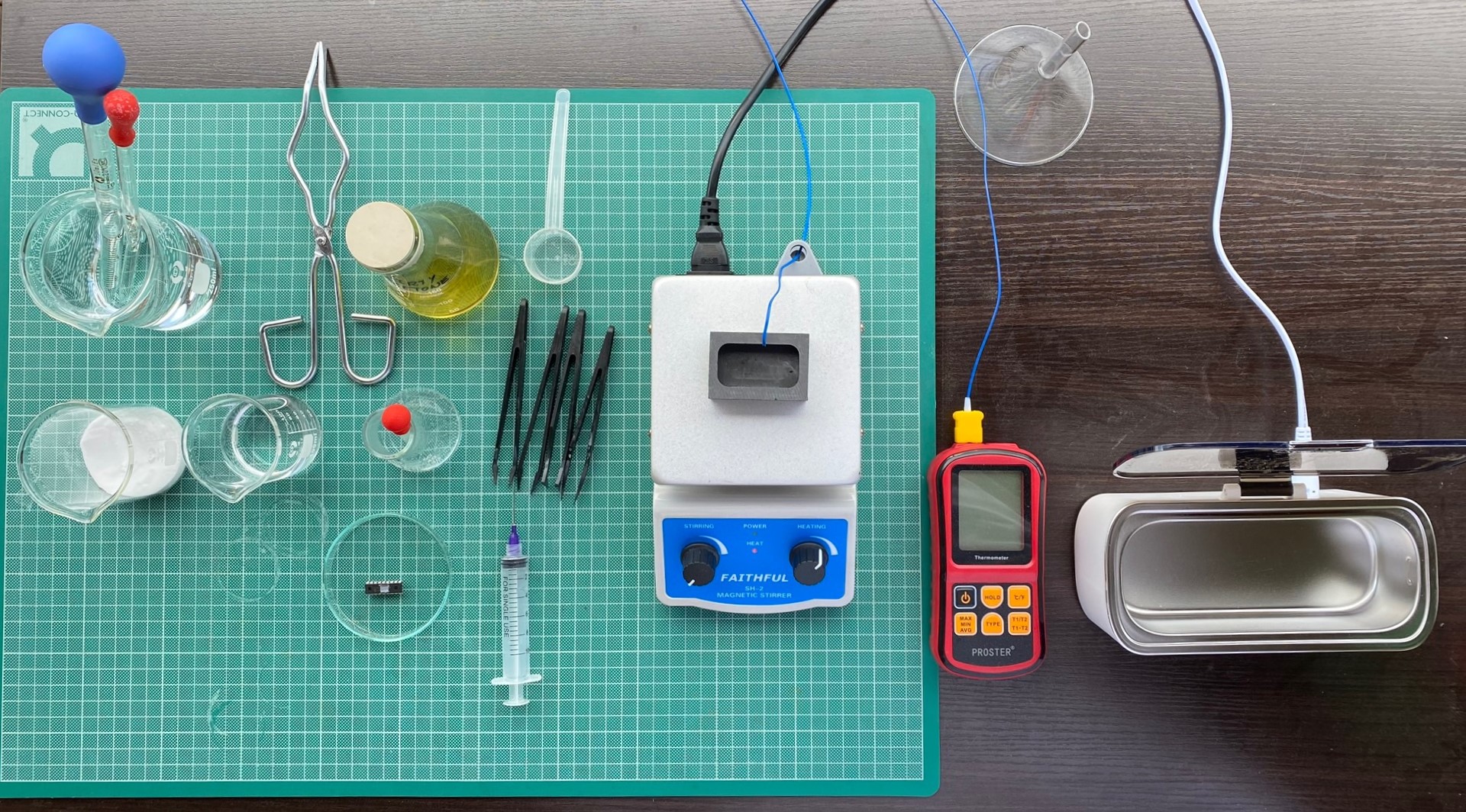
Tools and materials
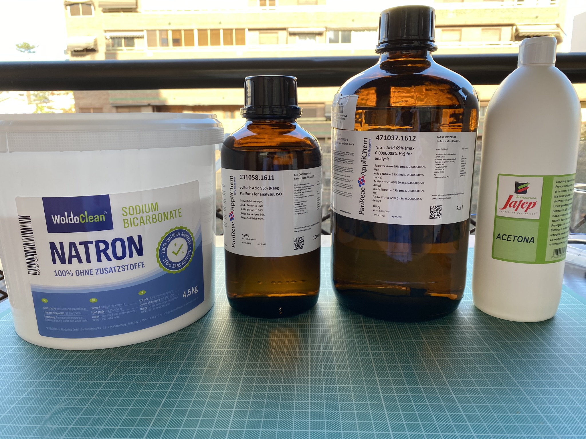
Chemicals I used during my experiments:
- Concentrated (69%) Nitric Acid
- 100% Sodium bicarbonate - Bought on Amazon
- 98% methanol - From a hardware store
- Acetone - From a hardware store
- Water - Either tap water or regular distilled water from a grocery store
I also ran a couple of tests using Sulfuric Acid, both standalone and mixed with the Nitric, but the results were not very promising. Probably because of the encapsulation material used in my ICs. These are the acids I used:
Necessary equipment:
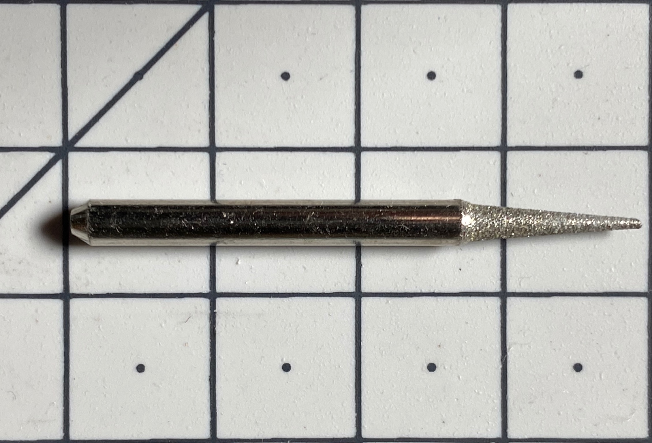
- Dremel
- I’ve found this off-brand pointy diamond bit to work great
- Hot plate
- High-temperature and acid safe recipient
- Tried using ceramic recipients and they worked well enough, but it was hard to maintain a stable temperature outside using my hot plate
- Graphite ingot molds ended up being better at conducting heat (hence maintaining a reasonably stable temperature outside) and providing easy access to the IC inside
- Plastic tweezers
- A syringe, or preferably an assortment of them
Other very useful equipment:
- An Erlenmeyer flask to keep a small amount of acid in a stable container
- Pipettes:
- 10ml pipette to transfer acid from its primary container to the flask
- 1ml pipette to drop acid on the ICs
- Beakers:
- A small one for acetone
- A large one for water, to rinse tools
- Thermocouple to monitor the temperature of the hot plate and IC container
- Tongs to move the hot ceramic/graphite container
- Ultrasonic cleaner. Explained later
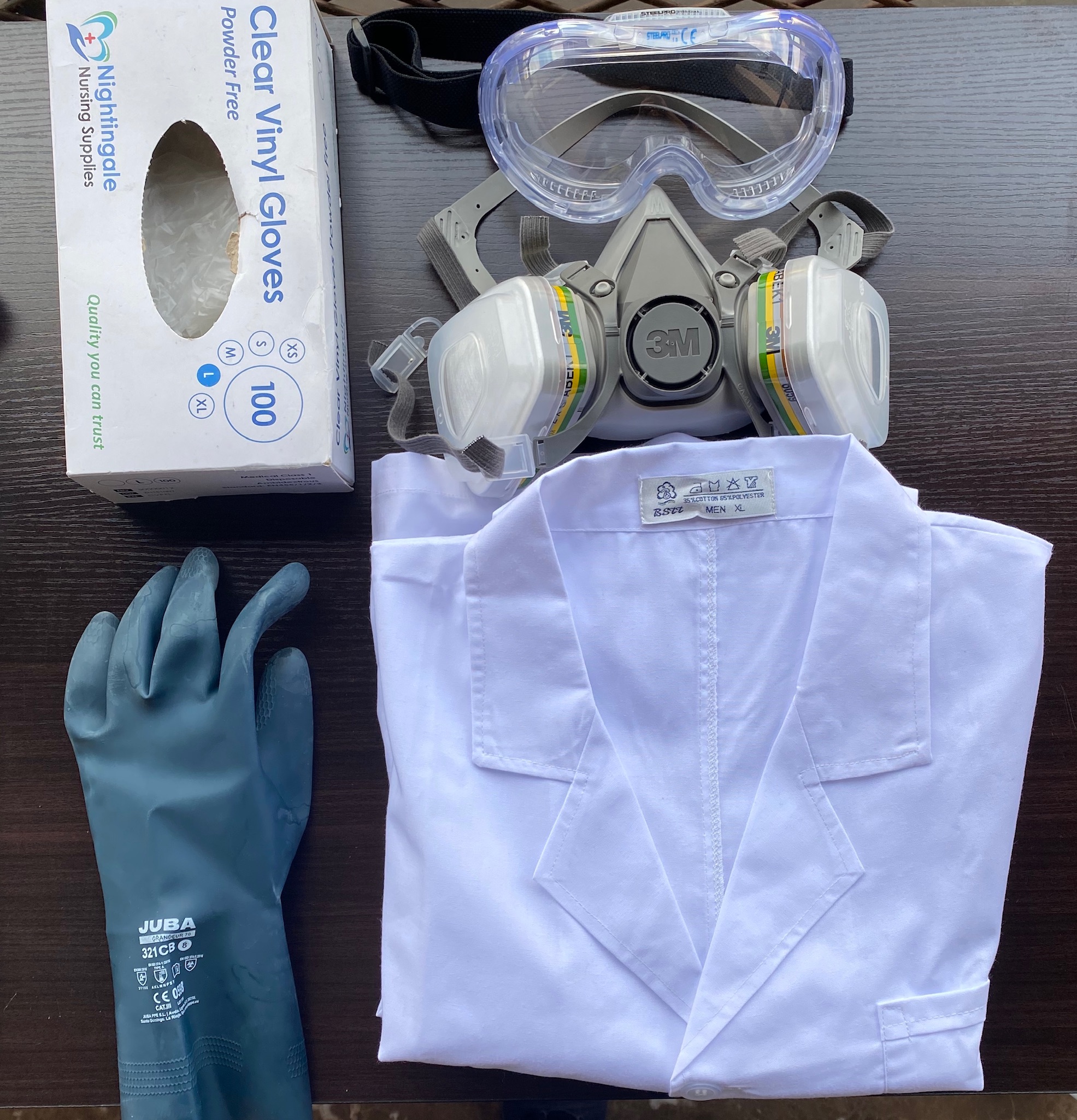
This picture shows most of the equipment used for the most successful method:
Attempt 1: Sand down the epoxy packaging
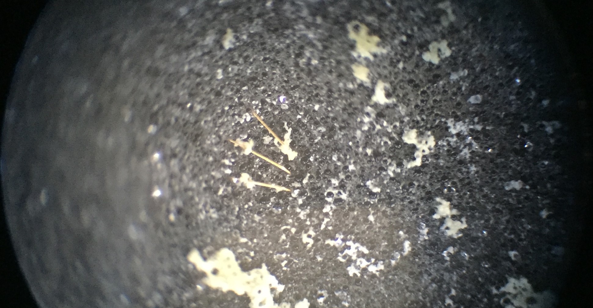
This is how the project started. I just got a new microscope, met with a couple of good friends, and we started looking at some random samples. Blood, dust, etc.
Then we decided to take a look at some random IC. We were not looking to see anything useful or complete; just an overall image of the silicon die in an IC, so I sanded down a microcontroller and we took a look. The result, as expected, was absolute garbage:
Well, that went exactly as terribly as expected… Time to go down the rabbit hole.
Attempt 2: Dremel + 69% Nitric Acid + Gentle acetone bath
Steps:
- Drill a pocket on the top of the epoxy package so the acid does not spill over to the leads.
- Place IC on a ceramic or graphite recipient, on top of the hot plate. Attach a thermocouple to the recipient to monitor its temperature
- When the temperature is appropriate (around 100 degrees C), drop one or 2 drops of acid in the epoxy pocket we just drilled. Wait until there is no more acid, and continue to apply acid when that happens
- Every once in a while, grab the IC with plastic tweezers, dip it in acetone and move it around to remove the reacted epoxy
Results: Terrible
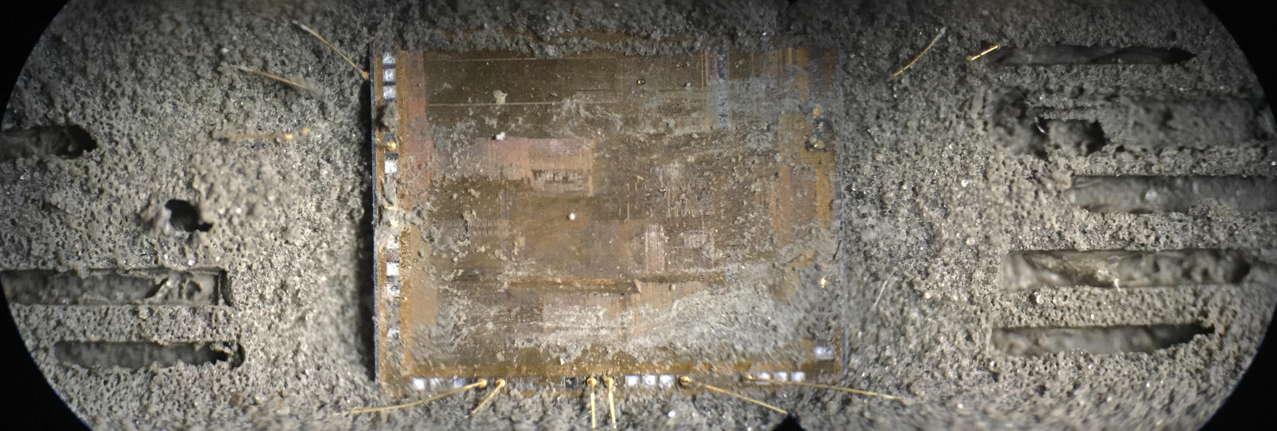
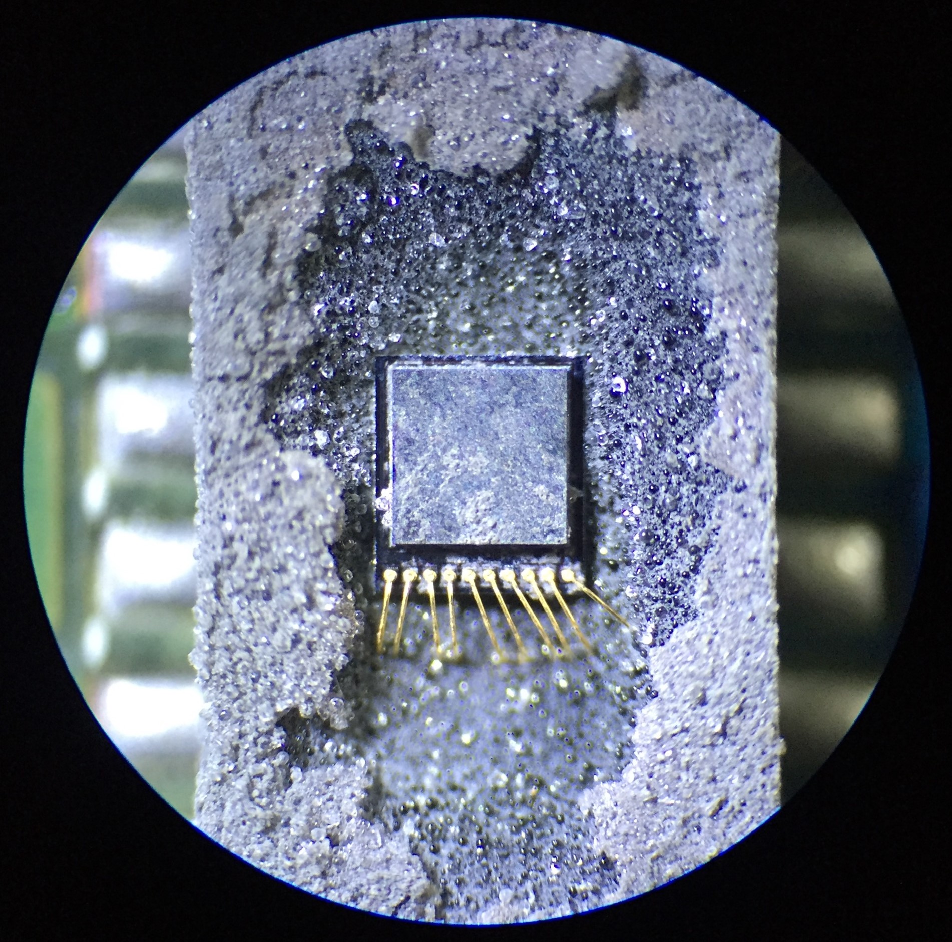
A simple acetone bath and some stirring are not enough to remove any significant amount of reacted epoxy packaging. After a while of carefully following this process, I ended up losing my patience. That eventually resulted in applying too much acid, spilling it over the IC’s leads, and melting them off. Then all bets were off, so I just kept applying acid until the IC was embarrassingly destroyed:
Reacted epoxy had a similar consistency to wet charcoal, so I could easily remove it with the tip of my tweezers. In a second test, that worked fine for a bit; until I encountered the die and ripped all the bonding wires right off it.
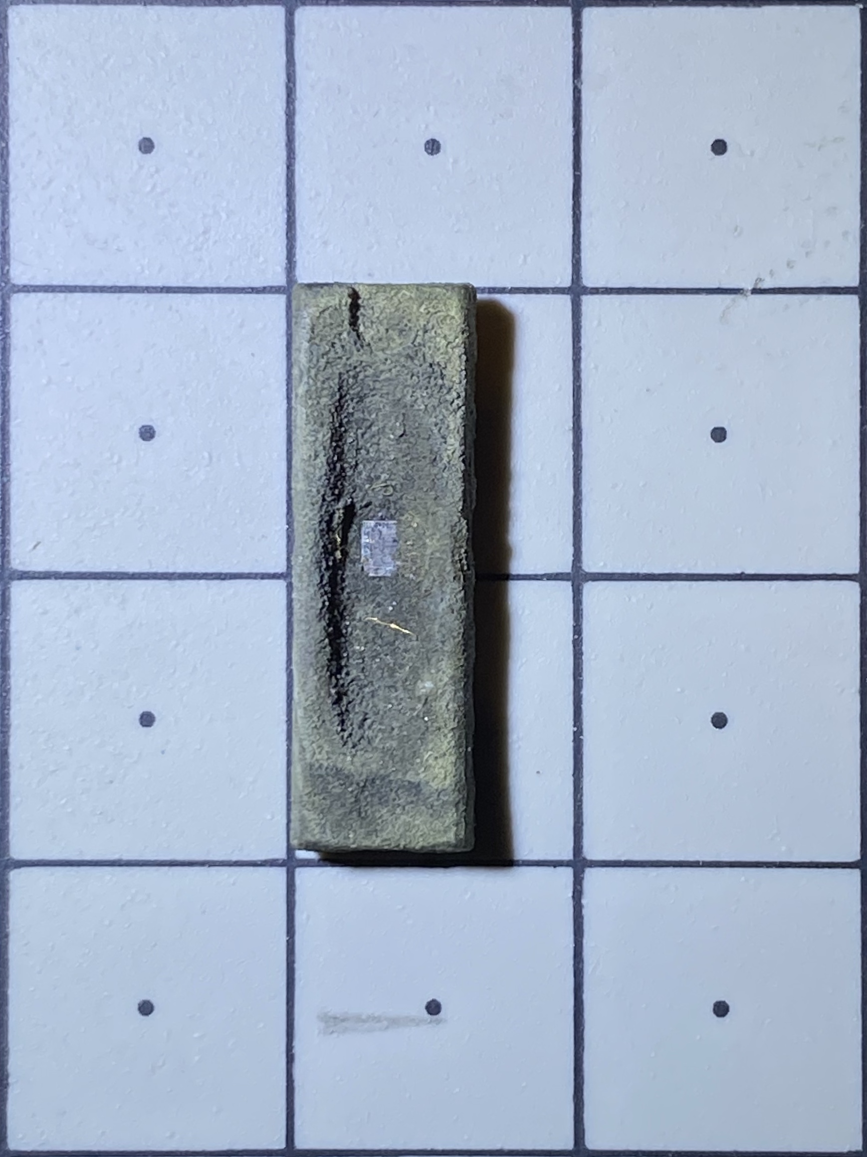
For a third attempt, I exercised patience and spent hours and hours applying acid to decap a simpler IC. It worked well enough:
That being said, spending an entire afternoon in PPE and constant tedious work for only a chance to get an undamaged IC is unacceptable to me.
I tried magnetically stirring the acetone bath in an attempt to accelerate the process while remaining reasonably gentle, but it made no significant difference.
I need a better method to remove the reacted epoxy.
Attempt 3: Dremel + 69% Nitric Acid + Acetone Syringe
After the previous failure, it seemed obvious I needed a method to remove more of the reacted epoxy without using a hard tool to manually extract it. I decided to push a stream of acetone aimed directly at the target area.
To avoid splashing acetone all over myself, I first submerged the IC in the acetone bath, and pushed the stream underneath the surface:
The process was significantly more effective, removing epoxy more precisely and at a much quicker rate. It still took a long time, but the syringe was a bit too effective in a sense…
The high-pressure stream pulled too much reacted epoxy off the IC, creating a wider, deeper hole much more rapidly. Soon enough, I was able to reach the top of the bond wires, hence locating the die. But the bond wires are akin to steel rods in reinforced concrete: they improve the robustness of the epoxy area atop of the silicon die.
By attempting to use the syringe method to extract the last area of epoxy over the die, it’s easy to first expose the internal parts of the leads surrounding it. Once that happens, and we apply more nitric acid, it will dissolve the leads faster than it weakens the epoxy atop of the die. The result is an unusable IC due to the disconnection of bond wires to its leads:
You’ll notice this happening before you actually dissolve the leads, because the acid reaction will be apparently different and more fuming, and the acid will quickly turn green-ish.
The workaround for this problem is rather simple: We need to minimize the size of the reacted area. We can easily achieve that by drilling a smaller and deeper pocket with the Dremel, directly over the silicon die.
- Locate the position and depth of the silicon die
- We could achieve this non-destructively with an X-Ray machine, but having a second identical IC to destroy with a Dremel and/or acid will work well enough
- Mark the position of the silicon die on the top of the target IC and dig as deep as you can with the Dremel without damaging the bond wires or the die
- Follow the same acid+acetone syringe procedure explained before
Drilling as deep as possible without damaging the IC is tricky. It’s easy to overshoot and end up with a damaged die:
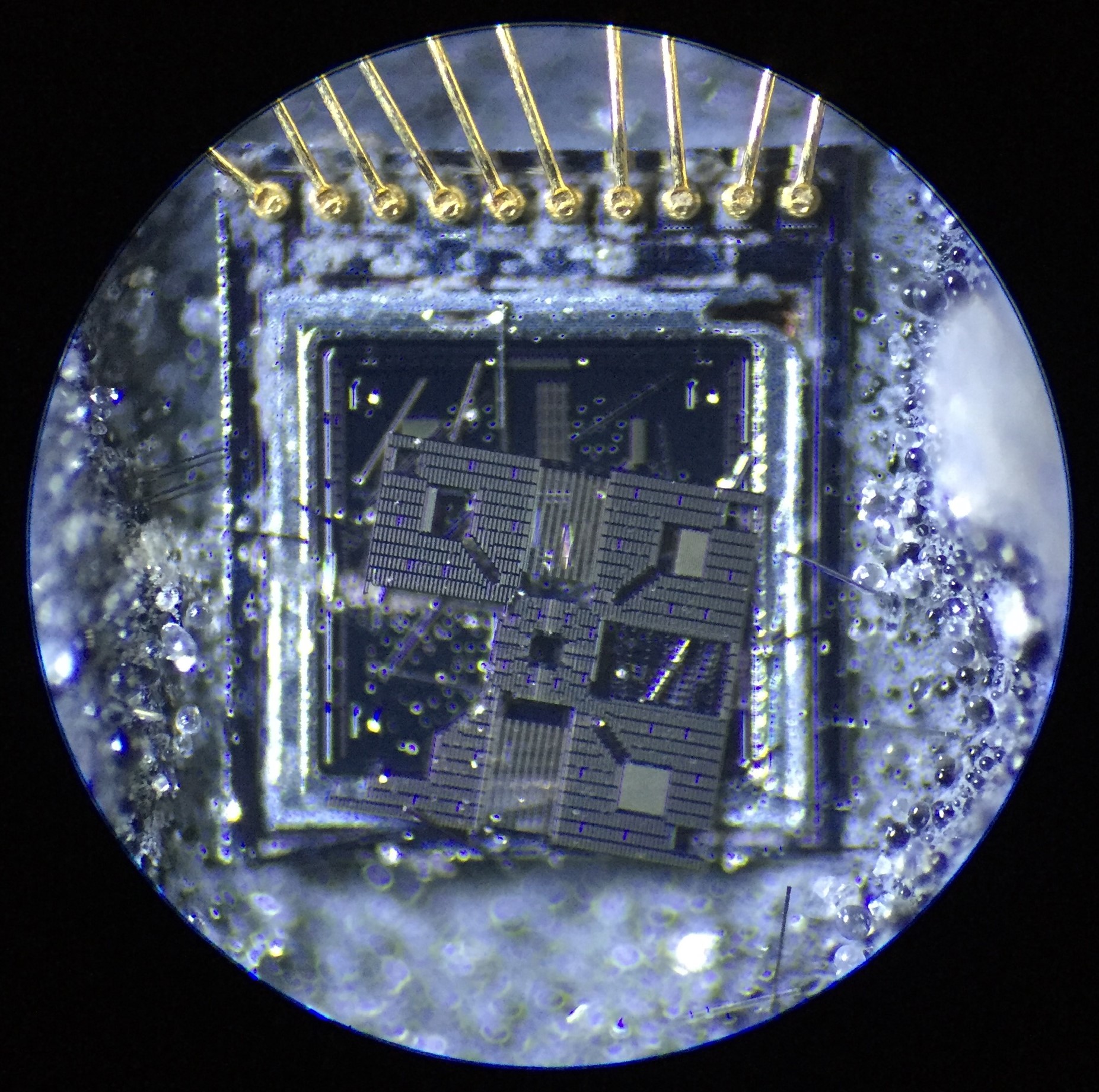
But once you get that part right, the results are quite decent:
Still, as you can see, most of the wire bonds are detached from the die. That’s almost definitely caused by the excessive acetone pressure exerted through the syringe when removing the last layer of epoxy off the die.
As you can see in the previous picture, there’s a lot of residues left over the silicon die. Trying to get as much as possible of the die is what resulted in excessive acetone pressure ripping the bonds off the die.
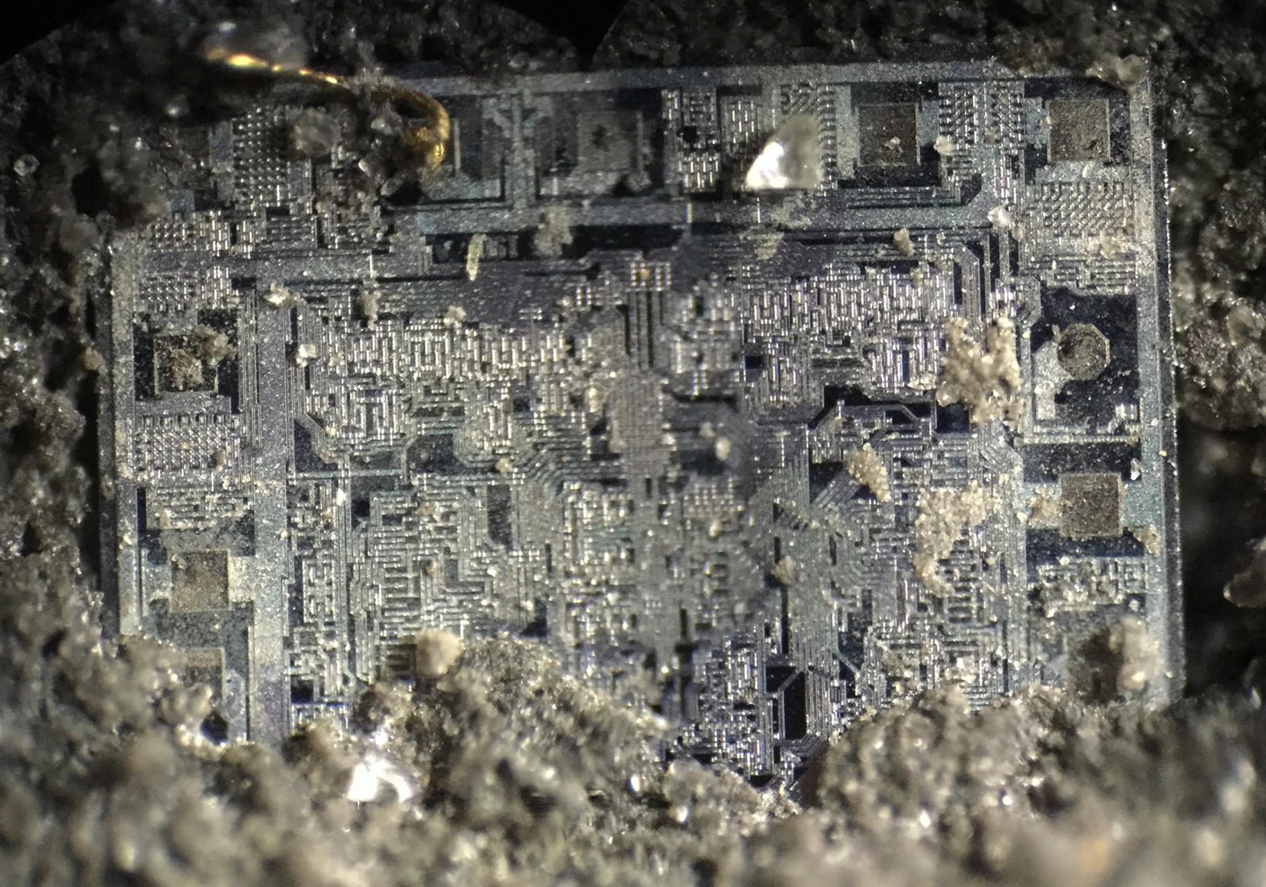
For complex ICs, where using increased magnification is necessary to discern more details, that residue will obstruct the view of the silicon die way too much. See:
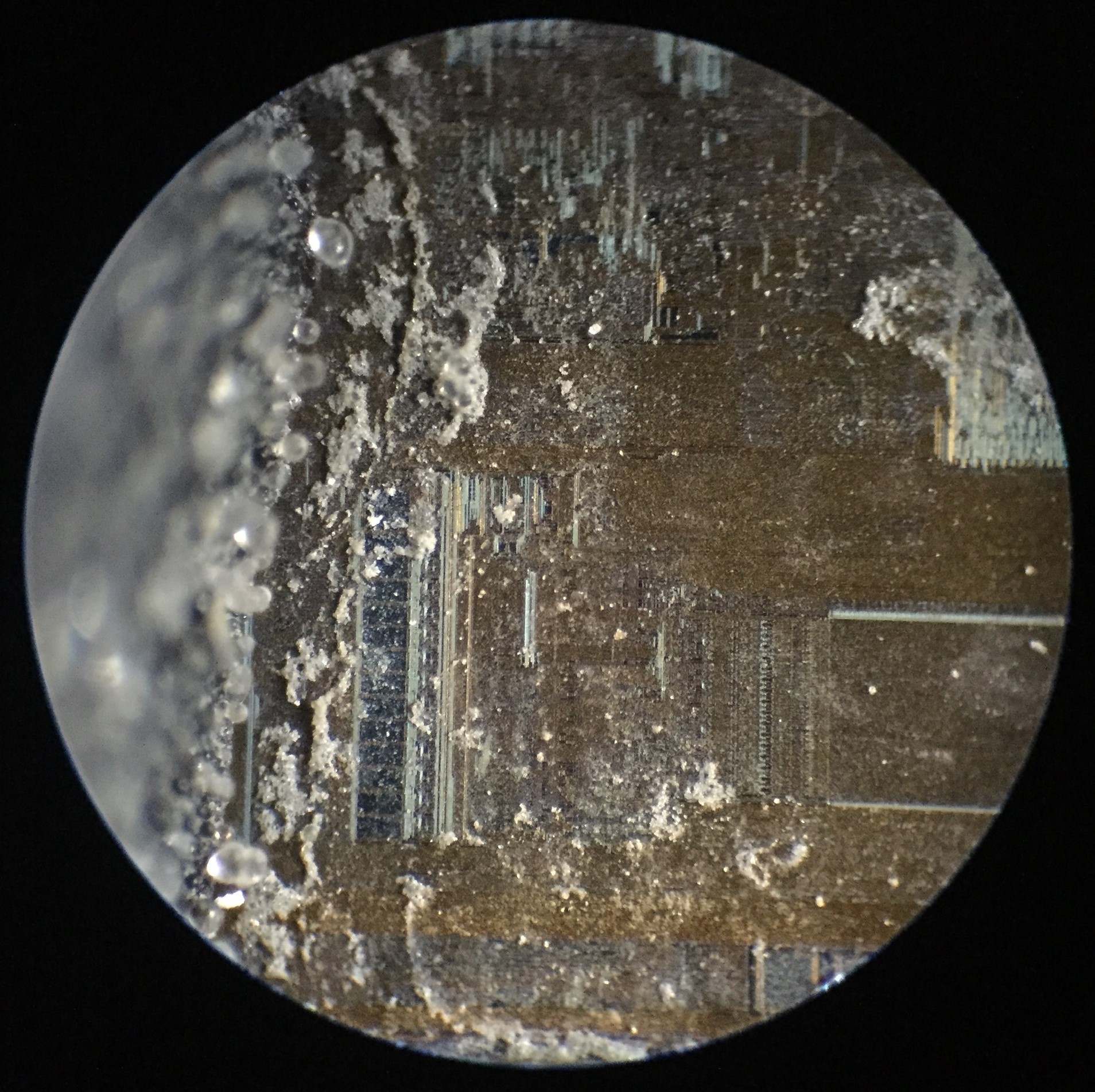
I’ve seen people get rid of such residue with their fingernails when using destructive decapsulation methods. Fingernails are supposedly hard enough to remove residue and soft enough not to damage the die. But that would obviously destruct the die bonds.
We need to figure out a better, gentler way to remove the last layer of epoxy and clean up residue off the silicon die without damaging the bonds.
Attempt 4: Dremel + 69% Nitric Acid + Acetone Syringe epoxy removal + Ultrasonic Methanol Cleanup
I’ve seen sources suggesting a pure methanol bath in an ultrasonic cleaning device to clean up the silicon die after the acid etching procedure. Let’s give it a try…
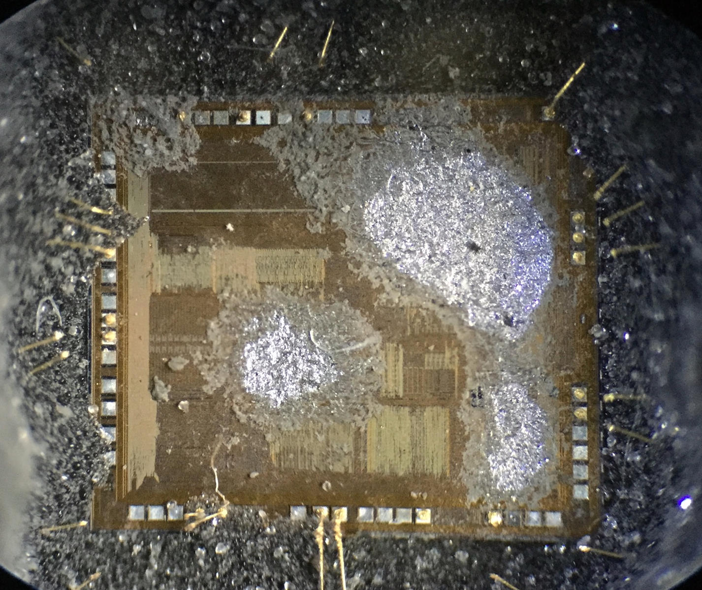
I bought a cheap ultrasound cleaning device off Amazon and tried using it to clean up the die in a methanol bath. It was able to remove a small part of the residue, and microscopic imaging seemed pretty successful immediately after bathing it for multiple minutes in separate attempts:
However, once the residue dries up again, most of the ingrained residue is still there:
This could be due to the cheap equipment I used, or the specific IC packaging and acids I used, but trying to replace methanol with acetone for the syringe procedure was also useless, so methanol is not gonna work for me.
Let’s try an acetone ultrasonic bath instead…
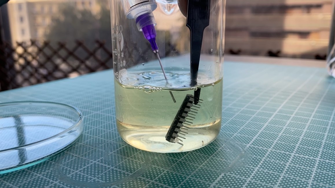
Attempt 5: Dremel + 69% Nitric Acid + Acetone Syringe + Ultrasonic Acetone Cleanup
First, once again, use the Dremel to drill a rather precise pocket over the silicon die
Use the Nitric deposition + Acetone syringe extraction method to dig through epoxy until the top of the bond wires are exposed
Once the bond wires are found and we’re about to reach the die, it’s time to stop using the acetone syringe method to extract reacted epoxy. Instead, submerge the IC in the ultrasonic acetone bath
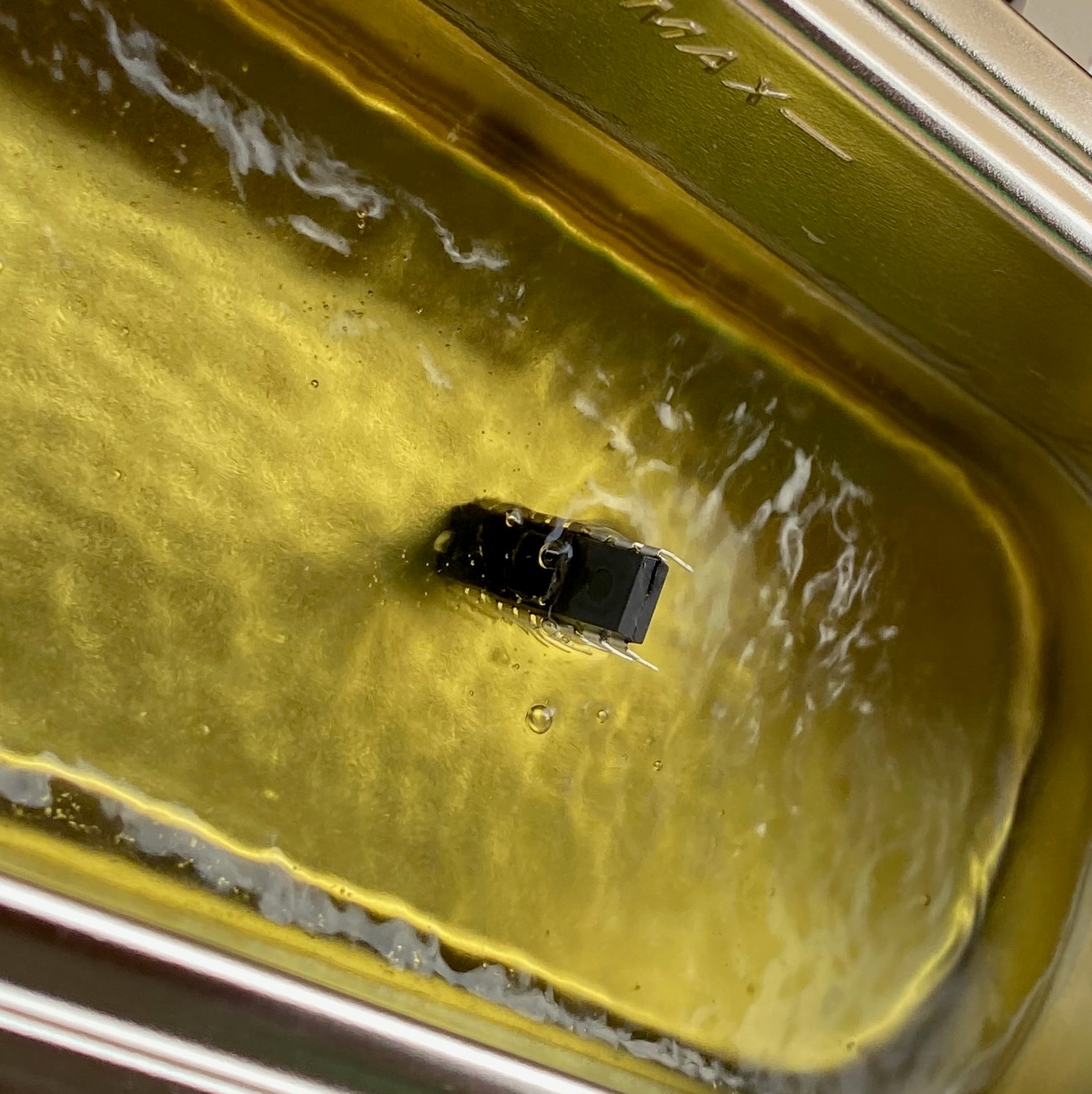
Repeat the acid deposition + acetone ultrasonic bath until the entire silicon die is exposed. If the ultrasonic bath is unable to get any particular chunk of epoxy, use a thin syringe to apply light pressure over that area.
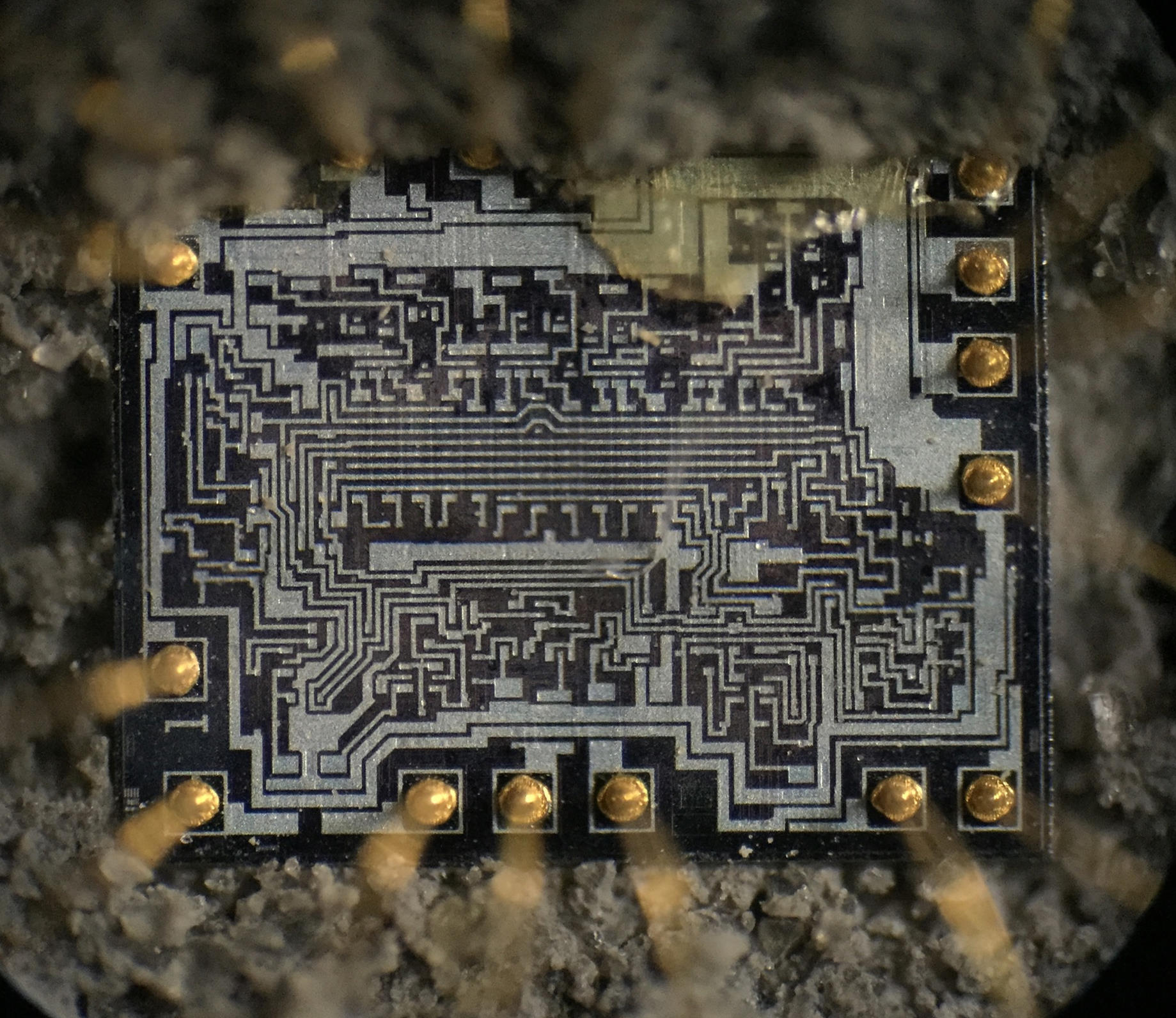
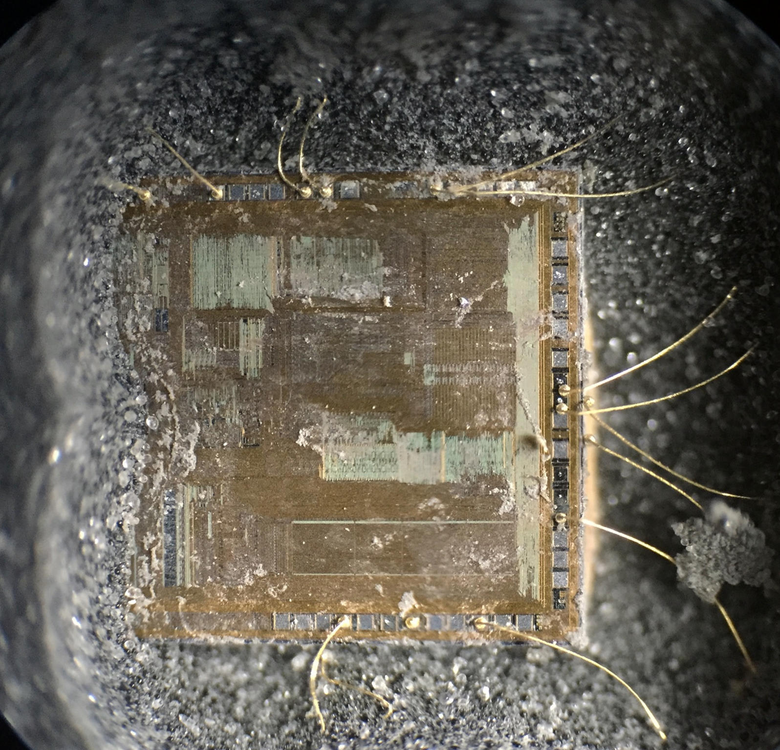
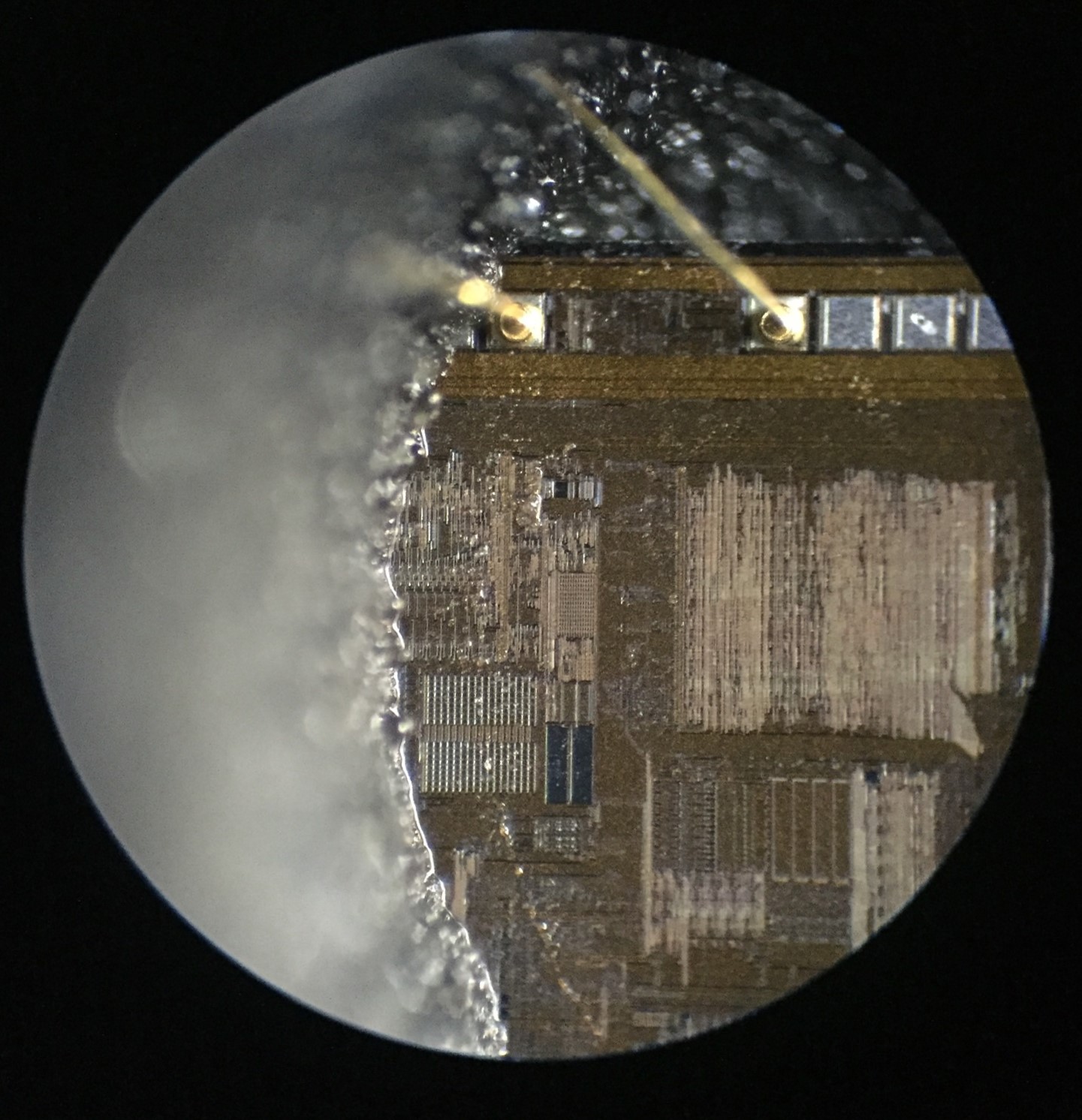
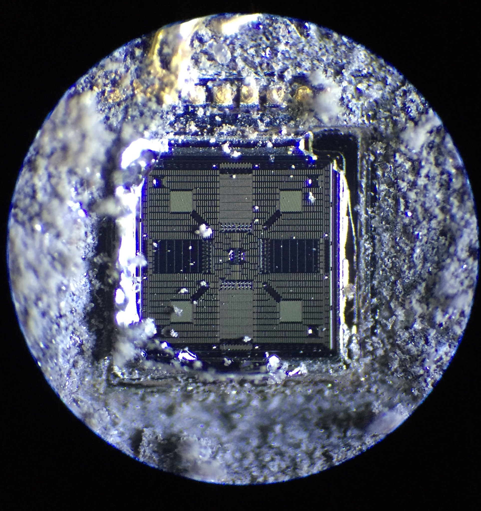
SUCCESS!
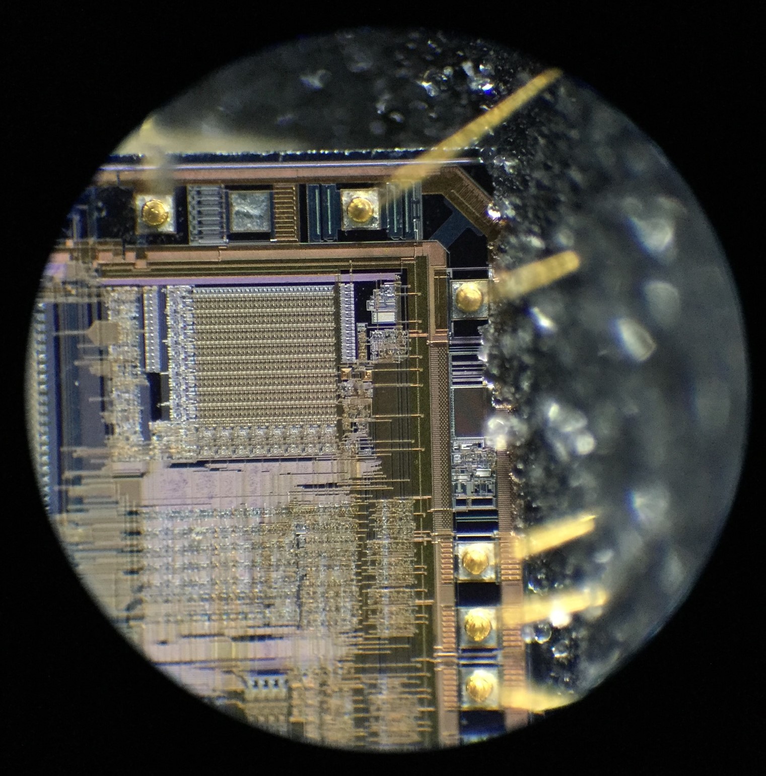
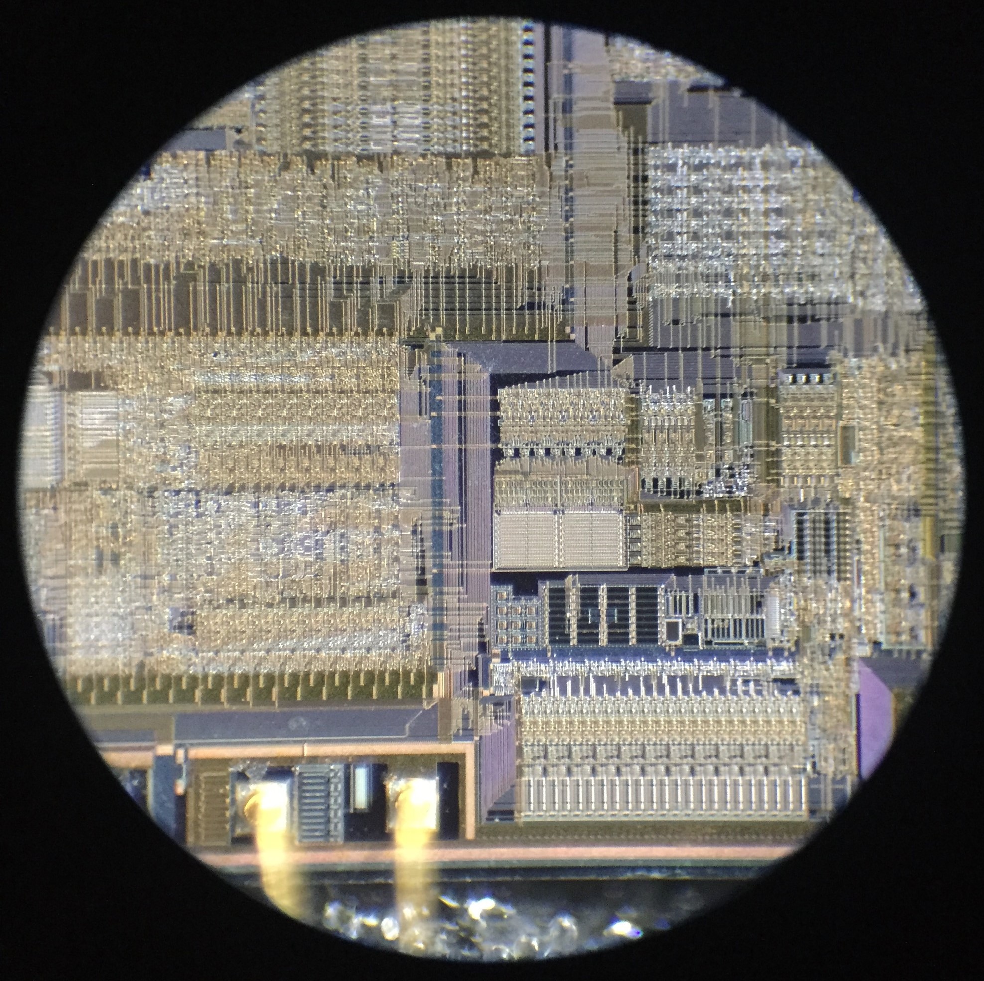
After all the previous attempts, this methodology was finally enough to non-destructively expose the entire silicon die. It worked on the first attempt, and the surface of the die was pristine right away. No messy residue obscuring the view under a microscope.
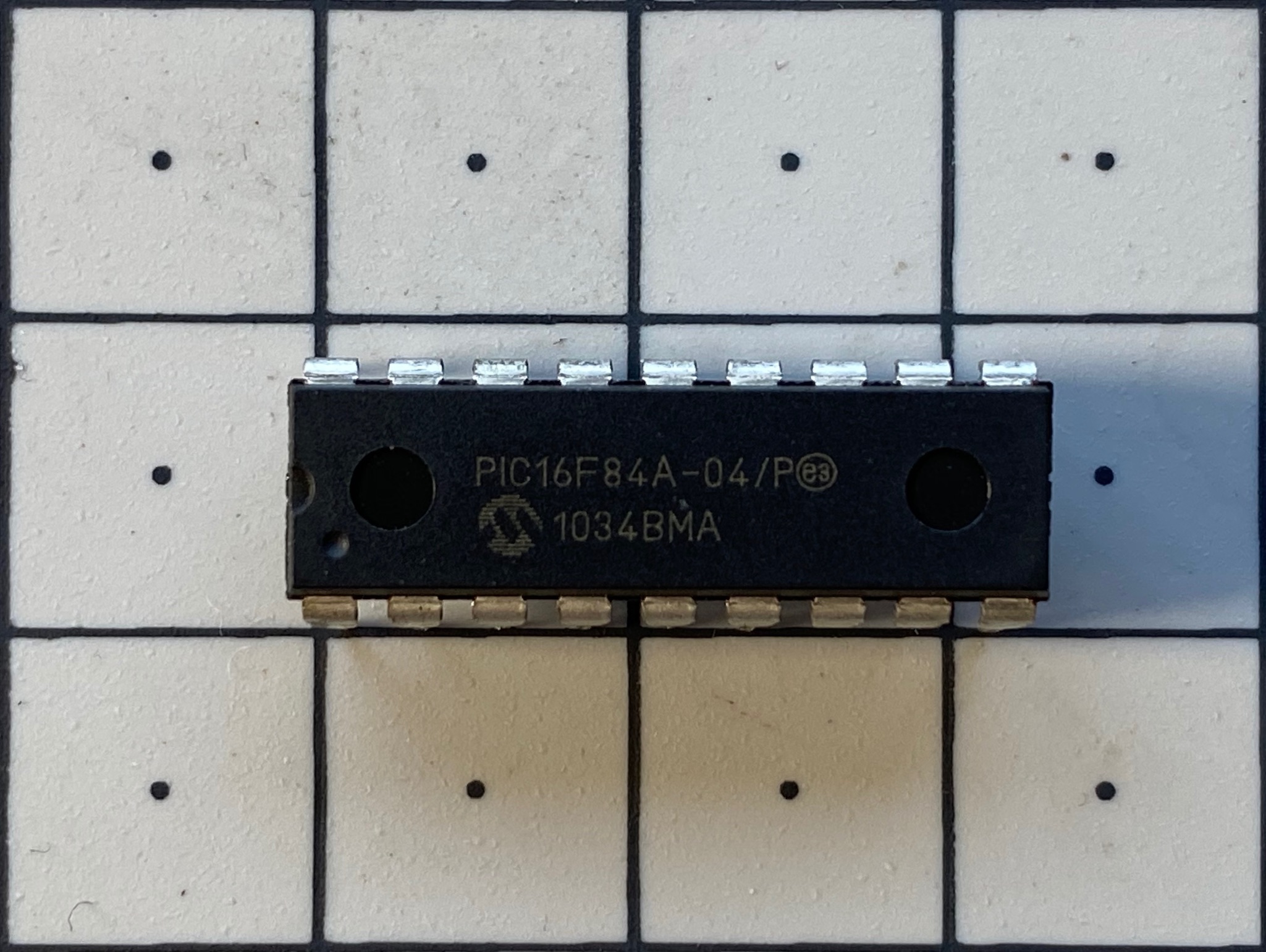
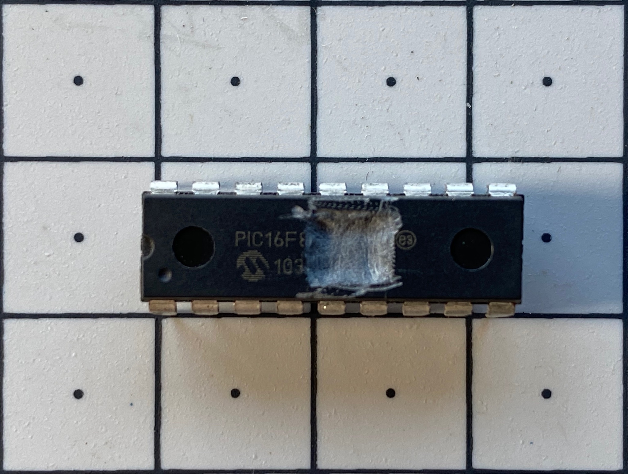
Let’s try with a more complex IC: a PIC16f84A.
Drill a pocket for the acid:
Apply acid on the hot plate:
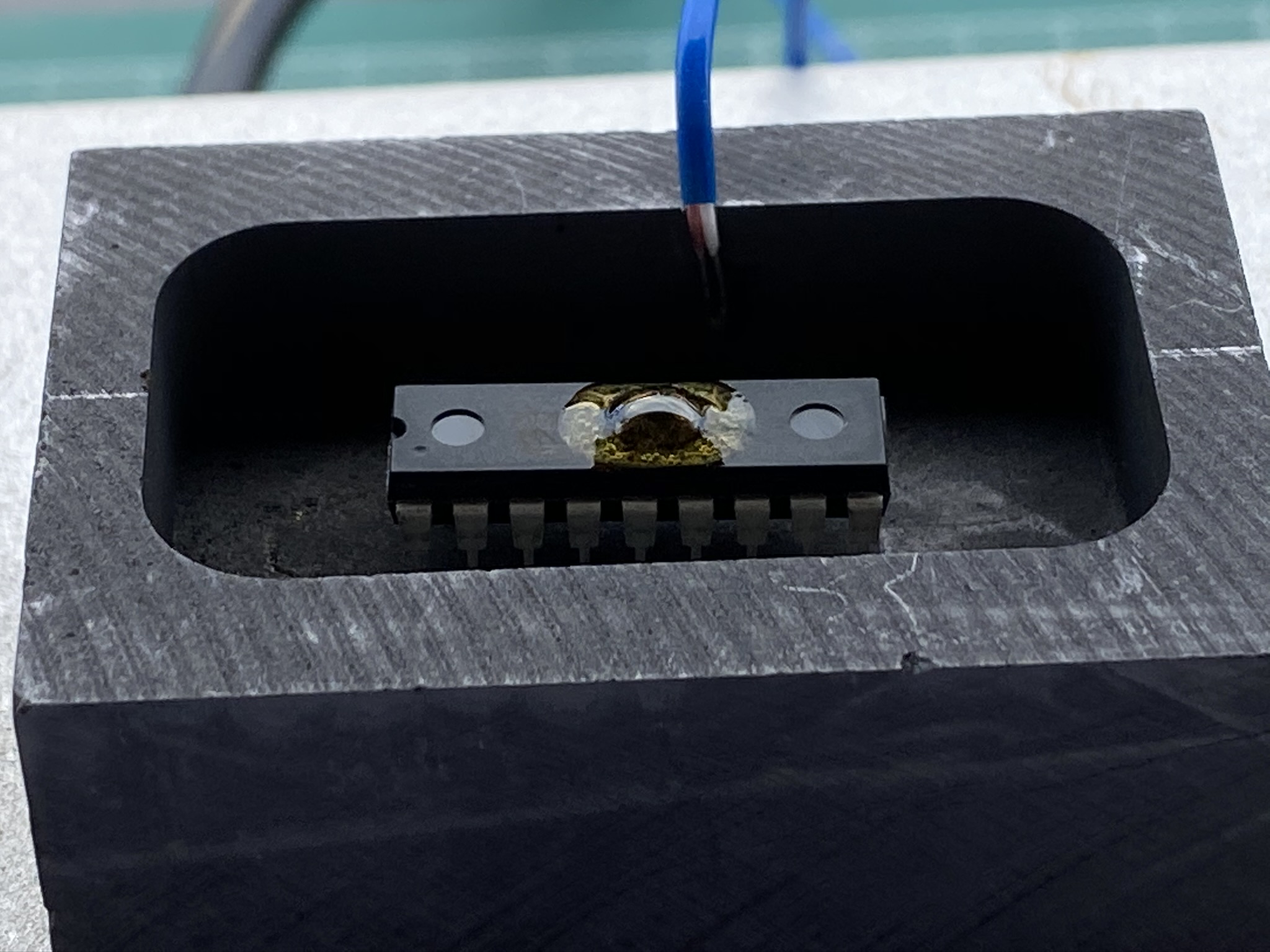
Extract reacted epoxy with the syringes and ultrasonic acetone bath, as explained earlier.
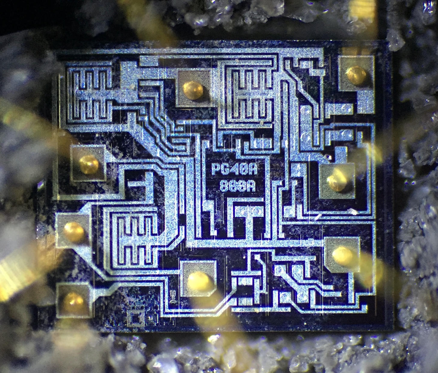
And, et voilà!
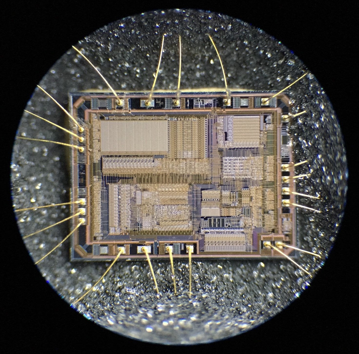
That’s the best result yet!
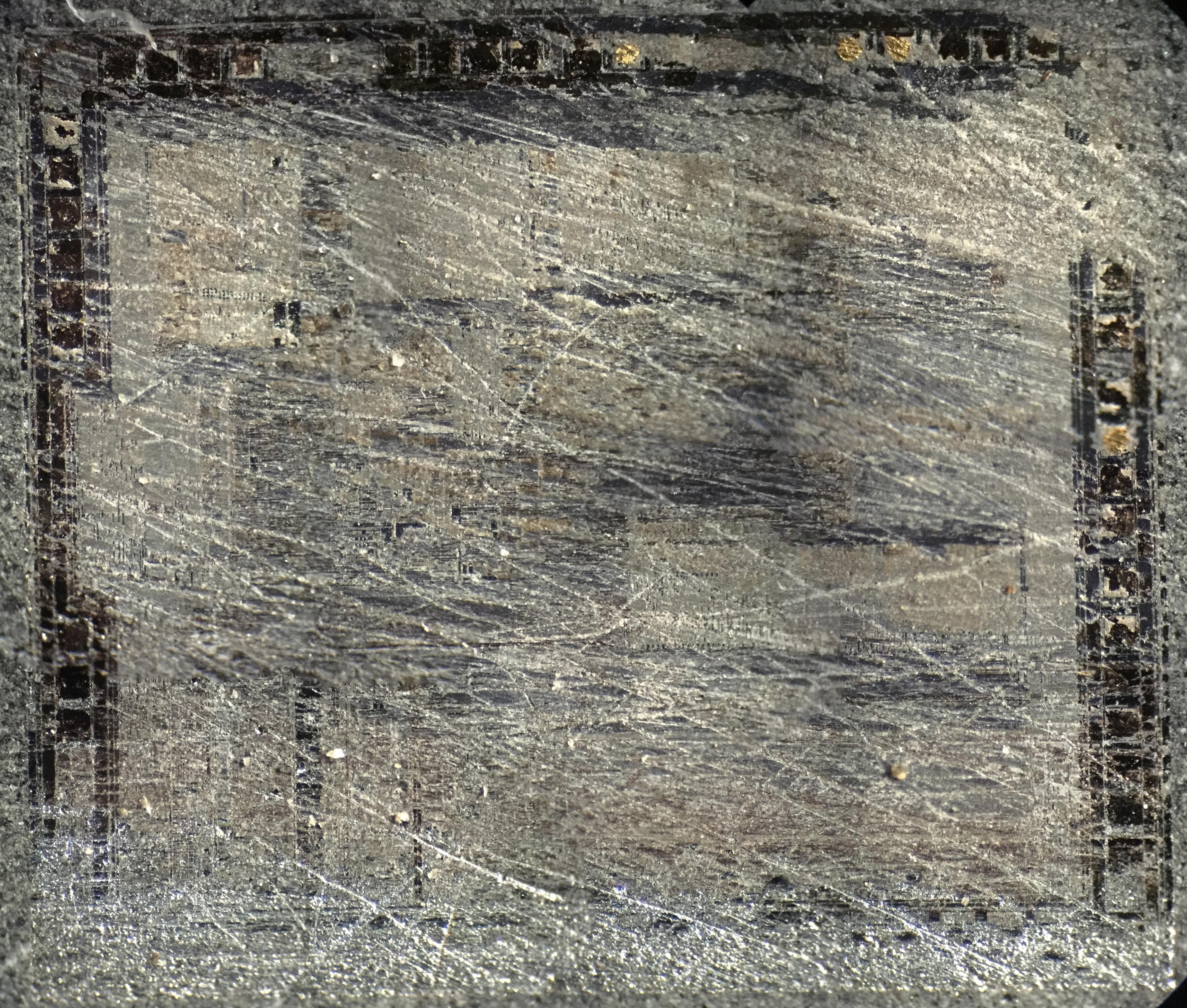
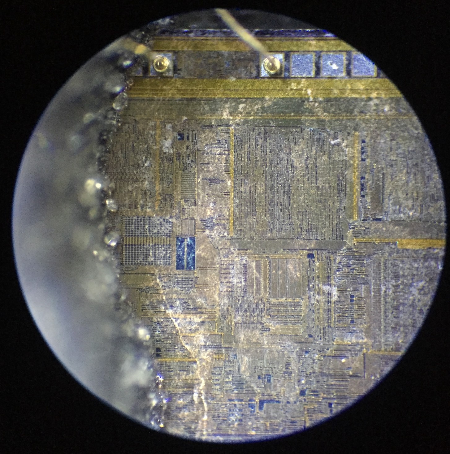
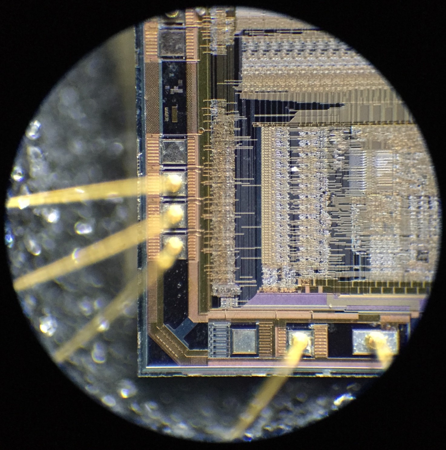
Here are some more details from the same IC:
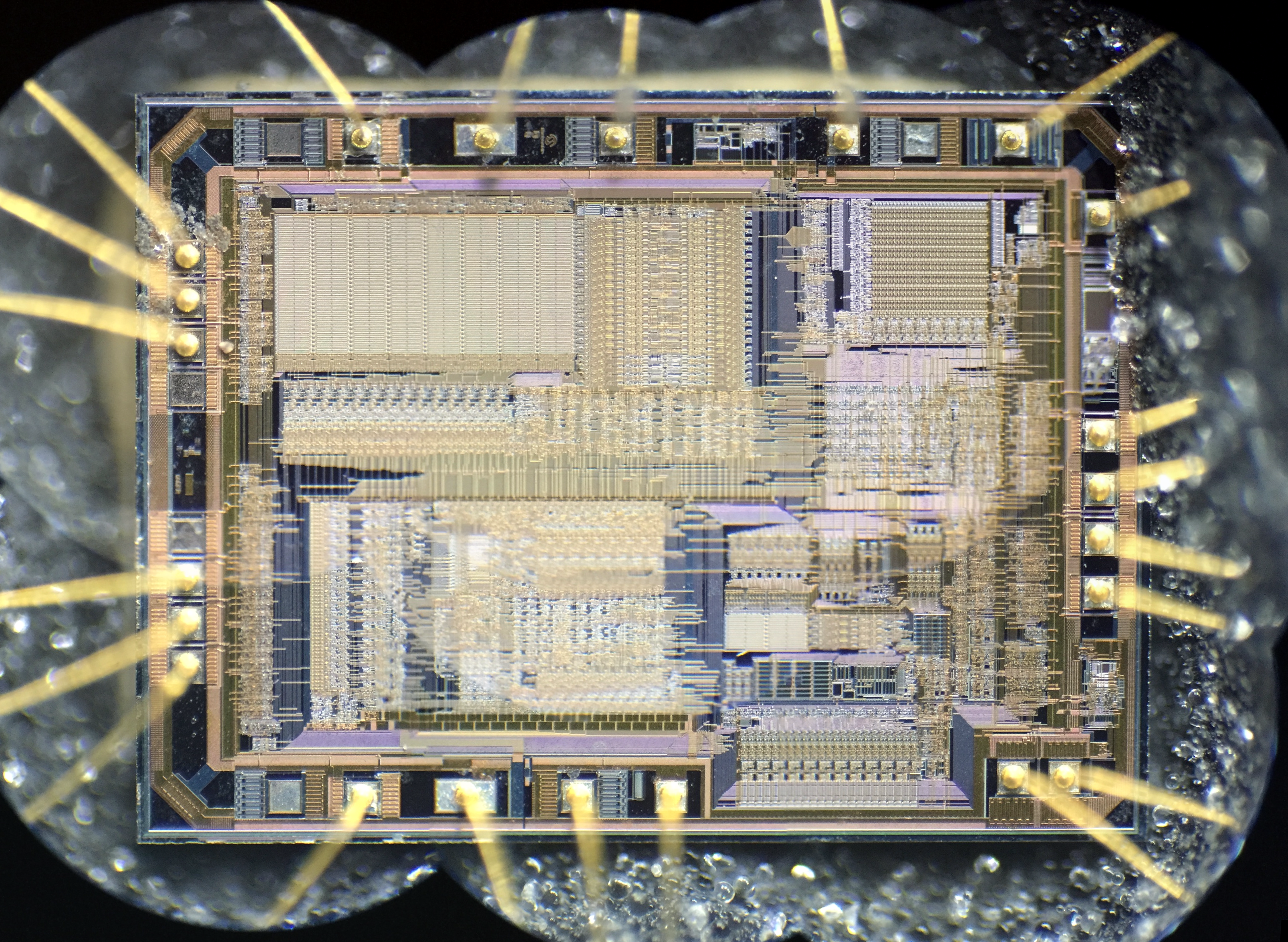
Taking great pictures under the microscope is not easy without expensive, specialized cameras. Getting the focus and lighting right throughout the sample is tricky, which makes it hard to get decent results from image stitching software. More info on imaging later.
Still, for the sake of gaining some more detail in the overall picture, here’s a composite image created from higher magnification pictures:
Attempt 6: Dremel + 69% Nitric Acid + Room temp Nitric Acid + Acetone Syringe + Ultrasonic Acetone Cleanup
I’ve seen different sources recommend a room temp nitric acid bath after the etching process. IIRC, the goal is to improve the uniformity of the etched area.
I tested it, and it didn’t make much of a difference. Perhaps it’s not that useful for manual deposition? I’m not sure, but given the lack of discernible differences, there’s no point for me to document it any further.
Attempt 7: Dremel + 98% Sulfuric Acid + 69% Nitric Acid + Ultrasonic Acetone Bath
I’ve seen a mix of sulfuric and nitric acid recommended in some literature. I did try it a couple of times, and it made no significant difference. It might help with different encapsulation or bond wire materials, but it was pretty much pointless in my tests.
I’d rather not deal with mixing dangerous acids, or the extra fuming it entails, so I gave up trying and would not recommend it unless pure Nitric is not doing the job.
Still, here’s one of the tests I ran. The methodology is identical to the previous attempt, only I mixed about 5ml of 98% Sulfuric Acid and 6.6ml of 69% Nitric Acid. That results in an approximate 50/50 mix of the active chemicals, accounting for the difference in purity.
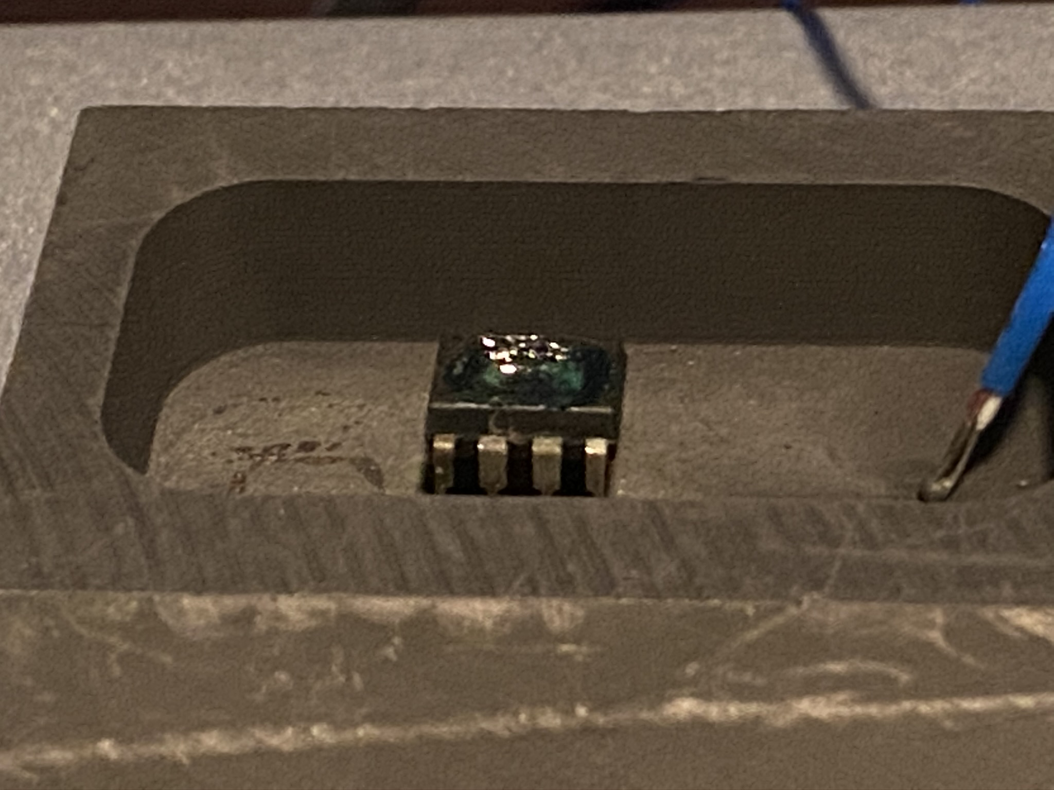
One of the tests I ran was on ADXL345 accelerometers, since I wanted to take a good look at a MicroElectroMechanical System (MEMS) IC. The IC itself is so small, I did not remove it from its development PCB so I could move it around more easily.
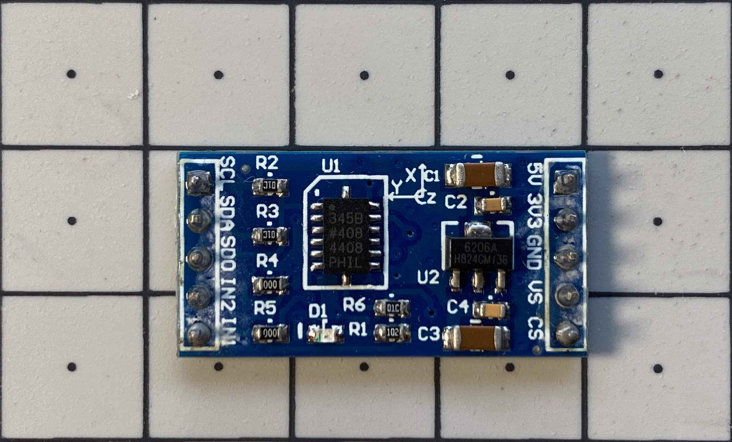
MEMS devices use micro-scale moving pieces, so they need to build differently. Let’s take a look…
Here we can see that the circuit’s internals are covered by a metal lid, so the epoxy does not glue the moving pieces together.
I first tried to remove the lid by pushing thin metallic tweezers from its side. In the process, I destroyed the upper layer of the MEMS:
I decapped another ADXL345, loaded a brand new blade on my X-Acto knife, and carefully cut through the lid’s edges using a USB “microscope” to see what I was doing. I cut through the wire bonds in the process, because I just cared about seeing the MEMS; not being non-destructive. Here’s the undamaged top layer of the accelerometer:
Looks great! I did not remove the residue for these pictures to avoid damaging the very delicate MEMS parts.
Taking Pictures Under the Microscope
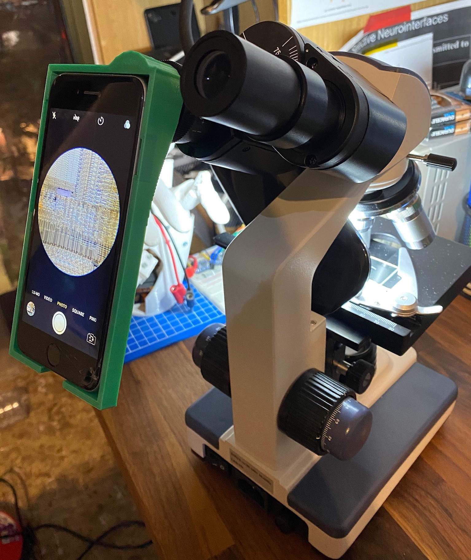
The ideal way to take pictures under the microscope would be to use a camera designed to fit into the microscope. I tried using a cheapish one included with the microscope I bought, but the results were pretty terrible; probably because lighting completely opaque samples like these is hard and imperfect in a microscope like mine.
Better cameras would definitely yield MUCH better results, but they are not cheap.
A good smartphone’s camera is better at handling poor/irregular lighting conditions, but aligning it to the eyepiece is terribly annoying and imprecise.
My solution was to design and 3D print an adapter to hold my old iPhone 6 directly aligned to the microscope’s lens. It’s not perfect, but it’s immensely better than everything else I tried.
Using this method, taking one decent picture of the IC is easy enough. But if we want a complete picture of the IC under higher magnification, we need to take multiple pictures and stitch them together. For that, I used Image Composite Editor, created by the Microsoft Research Computational Photography Group. Getting it to create good results was not without headaches and tediousness, but once it works, it does create pretty amazing results. I’d definitely recommend it.
Successful Imaging
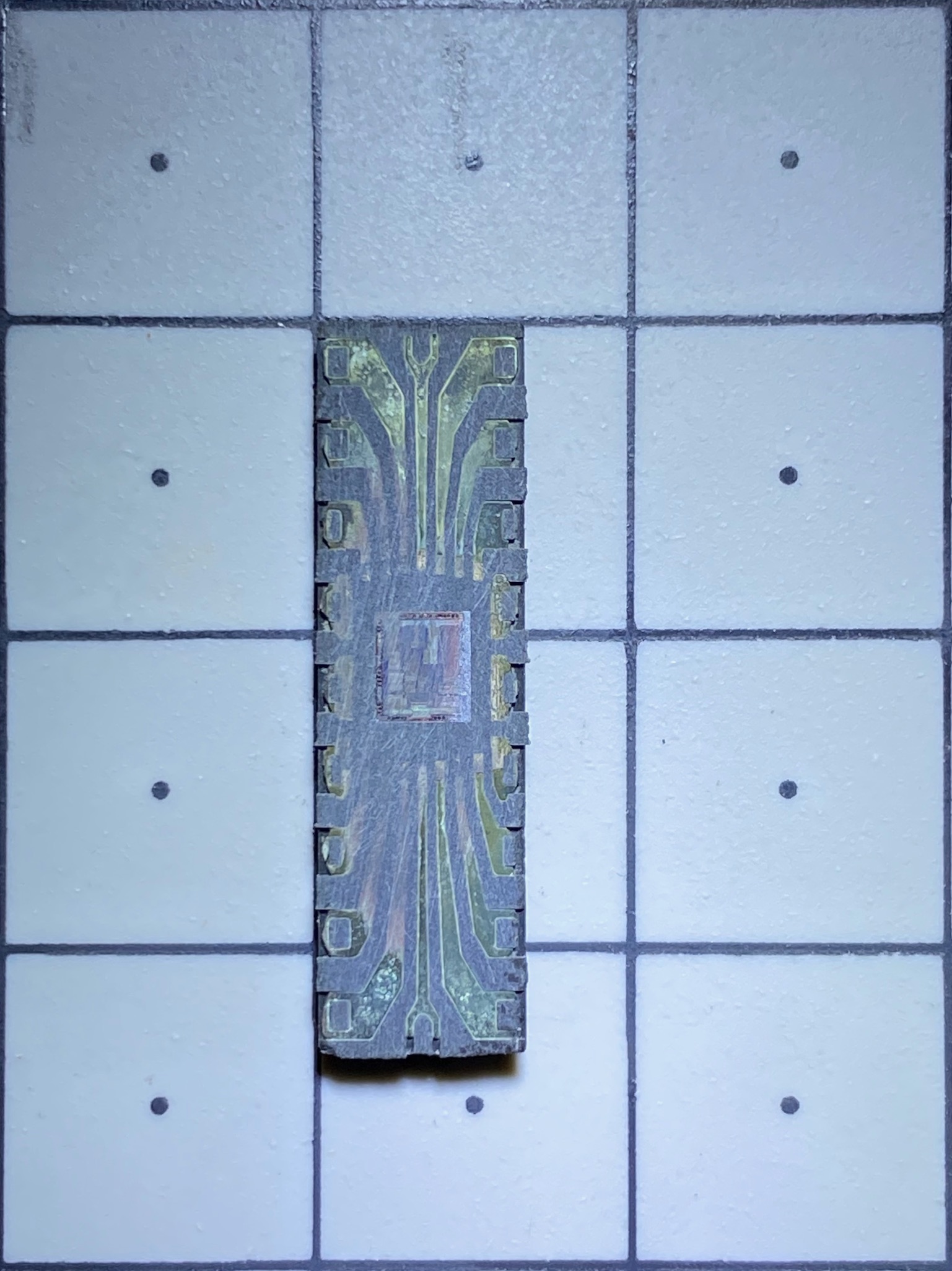
74LS48 BCD to 7 segment display decoder:
555 Timer:
Low magnification PIC16f84:
Composite image of PIC16f84:
ADXL345 accelerometer:
Resources
Papers:
- Acid Decapsulation of Epoxy Molded IC Packages With Copper Wire Bonds - DOI: 10.1109/TEPM.2006.882499
- Effective decapsulation of copper wire-bonded microelectronic devices for reliability assessment
Commercial documentation:
- Semitracks, Inc: Delid and decap
- Presto engineering: Wet chemical IC decapsulation
- Left Coast Instruments: Elite etch basic decapsulation process guide
- Samco partners in progress: Plasma Decap/Depassivation for IC Failure Analysis
- BSET EQ’s Plasma decapsulation equipment
Insightful research: